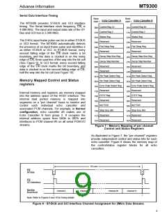
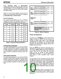
Advance Information
MT9300
Registers Description
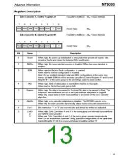
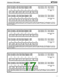
Echo Canceller A, Control Register A1
Read/Write Address: 00 + Base Address
H
7
6
5
4
3
2
1
0
Reset INJDis
BBM
PAD Bypass AdpDis
0
ExtDl
Reset Value:
00 .
H
Echo Canceller B, Control Register B1
Read/Write Address: 20 + Base Address
H
7
6
5
4
3
2
1
0
Reset INJDis
BBM
PAD Bypass AdpDis
1
0
Reset Value:
02 .
H
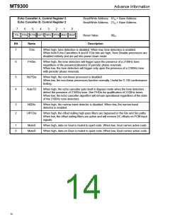
Bit
Name
Description
7
Reset
When high, the power-up initialization is executed which presets all register bits
including this bit and clears the Adaptive Filter coefficients.
6
5
INJDis
BBM
When high, the noise injection process is disabled. When low noise injection is
enabled.
When high the Back to Back configuration is enabled.
When low the Normal configuration is enabled.
Note: Do not enable Extended-Delay and BBM configurations at the same time.
Always set both BBM bits of the two echo cancellers (Control Register A1 and Control
Register B1) of the same group to the same logic value to avoid conflict.
4
3
PAD
When high, 12dB of attenuation is inserted into the Rin to Rout path.
When low the Rin to Rout path gain is 0dB.
Bypass
When high, Sin data is by-passed to Sout and Rin data is by-passed to Rout. The
Adaptive Filter coefficients are set to zero and the filter adaptation is stopped.
When low, output data on both Sout and Rout is a function of the echo canceller
algorithm.
2
AdpDis
0 or 1
When high, echo canceller adaptation is disabled. The MT9300 cancels echo.
When low, the echo canceller dynamically adapts to the echo path characteristics.
1
0
Bits marked as “1” or “0” are reserved bits and should be written as indicated.
ExtDl
or
When high, Echo Cancellers A and B of the same group are internally cascaded into
one 128ms echo canceller.
0
When low, Echo Cancellers A and B of the same group operate independently.
Note: Do not enable both Extended-Delay and BBM configurations at the same time.
Control Register B1 bit-0 is a reserved bit and should be written “0”.
13

 MITEL [ MITEL NETWORKS CORPORATION ]