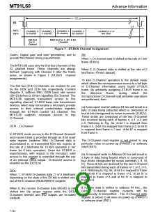
MT91L60
Advance Information
1
2
3
4
5
6
7
8
VBias
VRef
PWRST
M +
M -
20
19
18
17
16
15
14
13
12
11
VSSA
HSPKR +
HSPKR -
VDD
CLOCKin
STB/F0i
Din
IC
A/µ/IRQ
VSSD
CS
SCLK
DATA1
DATA2
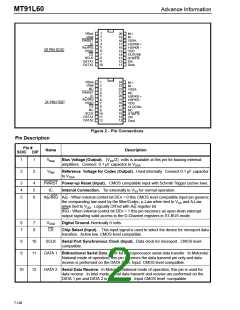
20 PIN SOIC
9
10
Dout
VBias
VRef
NC
24
23
22
21
20
19
18
17
16
15
14
13
1
2
3
4
5
6
7
8
M +
M -
VSSA
NC
HSPKR +
HSPKR -
VDD
CLOCKin
NC
STB/F0i
PWRST
IC
A/µ/IRQ
VSSD
CS
24 PIN PDIP
NC
9
SCLK
DATA1
DATA2
10
11
12
Din
Dout
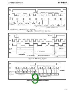
Figure 2 - Pin Connections
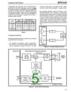
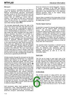
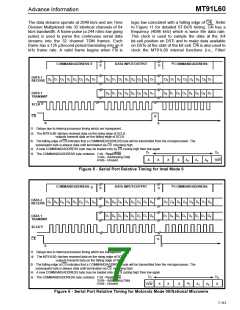
Description
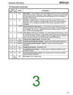
Pin Description
Pin #
Name
VBias
VRef
SOIC DIP
1
1
Bias Voltage (Output). (VDD/2) volts is available at this pin for biasing external
amplifiers. Connect 0.1 µF capacitor to VSSA
.
2
2
Reference Voltage for Codec (Output). Used internally. Connect 0.1 µF capacitor
to VSSA
.
3
4
5
4
5
6
PWRST Power-up Reset (Input). CMOS compatible input with Schmitt Trigger (active low).
IC Internal Connection. Tie externally to VSS for normal operation.
A/µ/IRQ A/µ - When internal control bit DEn = 0 this CMOS level compatible input pin governs
the companding law used by the filter/Codec; µ-Law when tied to VSS and A-Law
when tied to VDD. Logically OR’ed with A/µ register bit.
IRQ - When internal control bit DEn = 1 this pin becomes an open-drain interrupt
output signalling valid access to the D-Channel registers in ST-BUS mode.
6
7
7
8
VSSD
CS
Digital Ground. Nominally 0 volts.
Chip Select (Input). This input signal is used to select the device for microport data
transfers. Active low. CMOS level compatible.
8
9
10
11
SCLK
Serial Port Synchronous Clock (Input). Data clock for microport. CMOS level
compatible.
DATA 1 Bidirectional Serial Data. Port for microprocessor serial data transfer. In Motorola/
National mode of operation, this pin becomes the data transmit pin only and data
receive is performed on the DATA 2 pin. Input CMOS level compatible.
10
12
DATA 2 Serial Data Receive. In Motorola/National mode of operation, this pin is used for
data receive. In Intel mode, serial data transmit and receive are performed on the
DATA 1 pin and DATA 2 is disconnected. Input CMOS level compatible.
7-108

 MITEL [ MITEL NETWORKS CORPORATION ]