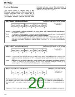
MT9092
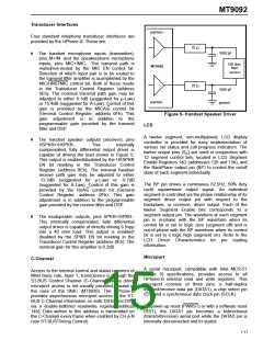
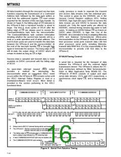
All data transfers through the microport are two-byte
transfers requiring the transmission of a Command/
Address byte followed by the data byte written or
read from the addressed register. CS must remain
asserted for the duration of this two-byte transfer. As
shown in Figure 6, the falling edge of CS indicates to
the HPhone-II that a microport transfer is about to
begin. The first 8 clock cycles of SCLK after the
falling edge of CS are always used to receive the
Command/Address byte from the microcontroller.
The Command/Address byte contains information
detailing whether the second byte transfer will be a
read or a write operation and of what address. The
next 8 clock cycles are used to transfer the data byte
between the HPhone-II and the microcontroller. At
the end of the two-byte transfer CS is brought high
again to terminate the session. The rising edge of CS
will tri-state the output driver of DATA1 which will
remain tri-stated as long as CS is high.
Lastly, provision is made to seperate the transmit
and receive data streams onto two individual pins.
This control is given by the DATASEL pin in the
General Control Register (address 0Fh). Setting
DATASEL logic high will cause DATA1 to become the
data receive pin and DATA2 to become the data
transmit pin. Only the signal paths are altered by
DATASEL; internal timing remains the same in both
cases. Tri-stating on DATA2 follows CS as it does on
DATA1 when DATASEL is logic low. Use of the
DATASEL bit is intended to help in adapting Motorola
(SPI) and National Semiconductor (Micro-wire)
microcontrollers to the HPhone-II. Note that whereas
Intel processor serial ports transmit data LSB first
other processor serial ports, including Motorola,
transmit data MSB first. It is the responsibility of the
microcontroller to provide LSB first data to the
HPhone-II.
ST-BUS/Timing Control
Receive data is sampled and transmit data is made
available on DATA1 concurrent with the falling edge
of SCLK.
A serial link is required for the transport of data
between the HPhone-II and the external digital
transmission device. The HPhone-II utilizes the ST-
BUS architecture defined by Mitel Semiconductor.
Refer to Mitel Application Note MSAN-126. The
HPhone-II ST-BUS consists of output and input
serial data streams, DSTo and DSTi respectively, a
synchronous clock signal C4i, and a framing pulse
F0i.
An open-drain interrupt request (IRQ) output
provides
a
method
for
interrupting
the
microcontroller when an unmasked HDLC event
occurs within the HPhone-II. IRQ remains active until
the HDLC Interrupt Status Register is read or a
(hardware/software) reset occurs. More detail is
provided in the section pertaining to the HDLC
functional block.
➃
COMMAND/ADDRESS
COMMAND/ADDRESS ➄
DATA INPUT/OUTPUT
➀
➀
DATA 1
Receive
D0 D1 D2 D3 D4 D5 D6 D7
D0 D1 D2 D3 D4 D5 D6 D7
D0 D1 D2 D3 D4 D5 D6 D7
DATA 1 or DATA 2
Transmit
D0 D1 D2 D3 D4 D5 D6 D7
D0 D1 D2 D3 D4 D5 D6 D7
➁
SCLK
CS
➃
➂
➂
➀
➁
Delays due to MCS-51 internal timing which are transparent.
The HPhone-II: -latches received data on the falling edge of SCLK
-outputs transmit data on the falling edge of SCLK
➂
The falling edge of CS indicates that a COMMAND/ADDRESS byte will be transmitted from the microprocessor. The subsequent
byte is always data followed by CS returning high.
A new COMMAND/ADDRESS byte may be loaded only by CS cycling high then low again.
➃
➄
D7
D0
The COMMAND/ADDRESS byte contains:
1 bit - Read/Write
0
A5
A4
A3
A2
A1
A0
R/W
6 bits - Addressing Data
1 bit - Not used, write logic "0"
Figure 6 - Serial Port Relative Timing
7-18

 MITEL [ MITEL NETWORKS CORPORATION ]