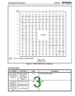
Advanced Information
CMOS MT90826
Locations in the connection memory are associated
with particular ST-BUS output channels. When a
channel is due to be transmitted on an ST-BUS
output, the data for this channel can be switched
either from an ST-BUS input in connection mode, or
from the lower half of the connection memory in
message mode. Data destined for a particular
channel on a serial output stream is read from the
data memory or connection memory during the
previous channel timeslot. This allows enough time
for memory access and parallel-to-serial conversion.
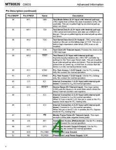
drivers and bit error test pattern enable. If an output
channel is set to a high-impedance state by setting
the OE bit to zero in the connection memory, the ST-
BUS output will be in a high impedance state for the
duration of that channel. In addition to the per-
channel control, all channels on the ST-BUS outputs
can be placed in a high impedance state by pulling
the ODE input pin low and programming the output
stand by (OSB) bit in the control register to low. This
action overrides the individual per-channel
programming by the connection memory bits. See
Table 2 for detail.
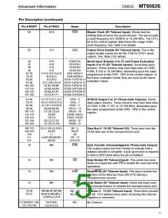
Connection and Message Modes
The connection memory data can be accessed via
the microprocessor interface through the D0 to D15
pins. The addressing of the device internal registers,
data and connection memories is performed through
the address input pins and the Memory Select (MS)
bit of the control register.
In the connection mode, the addresses of the input
source data for all output channels are stored in the
connection memory. The connection memory is
mapped in such
a
way that each location
corresponds to an output channel on the output
streams. For details on the use of the source
address data (CAB and SAB bits), see Table 18.
Once the source address bits are programmed by
the microprocessor, the contents of the data memory
at the selected address are transferred to the
parallel-to-serial converters and then onto an ST-
BUS output stream.
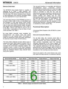
Clock Timing Requirements
The master clock (CLK) frequency must be either at
8.192 or 16.384MHz for serial data rate of 2.048,
4.096, 8.192 and 16.384Mb/s; see Table 6 for the
selections of the master clock frequency.
By having several output channels connected to the
same input source channel, data can be broadcasted
from one input channel to several output channels.
Switching Configurations
The MT90826 maximum non-blocking switching
configurations is determined by the data rates
selected for the serial inputs and outputs. The
switching configuration is selected by three DR bits
in the control register. See Table 5 and Table 6.
In message mode, the microprocessor writes data to
the connection memory locations corresponding to
the output stream and channel number. The lower
half (8 least significant bits) of the connection
memory content is transferred directly to the parallel-
to-serial converter. This data will be output on the
ST-BUS streams in every frame until the data is
changed by the microprocessor.
8Mb/s mode (DR2=0, DR1=0, DR0=0)
When the 8Mb/s mode is selected, the device is
configured with 32-input/32-output data streams
each having 128 64Kbit/s channels. This mode
allows a maximum non-blocking capacity of 4,096 x
4,096 channels. Table 1 summarizes the switching
configurations and the relationship between different
serial data rates and the master clock frequencies.
The three most significant bits of the connection
memory controls the following for an output channel:
message or connection mode, constant or variable
delay mode, enables/tristate the ST-BUS output
ODE pin
OSB bit in Control register
OE bit in Connection Memory
ST-BUS Output Driver
0
X
1
0
1
0
X
0
1
1
X
0
1
1
1
High-Z
Per Channel High-Z
Enable
Enable
Enable
Table 2 - Output High Impedance Control
7

 MITEL [ MITEL NETWORKS CORPORATION ]