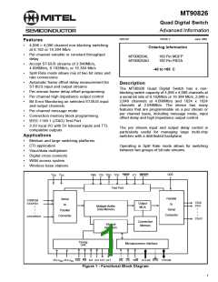
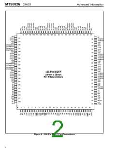
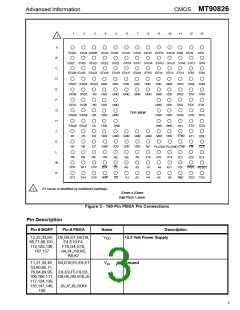
Advanced Information
CMOS MT90826
Pin Description (continued)
Pin # MQFP
Pin # PBGA
Name
Description
52
K13
CLK
Master Clock (5V Tolerant Input): Serial clock for
shifting data in/out on the serial streams. This pin accepts
a clock frequency of 8.192MHz or 16.384 MHz. The CPLL
bit in the control register determines the usage of the
clock frequency. See Table 6 for details.
55
J13
ODE
Output Drive Enable (5V Tolerant Input): This is the
output-enable control pin for the STo0 to STo31 serial
outputs. See Table 2 for details.
56
57
58
H13
H12
G13
STi0/FEi0,
STi1/FEi1
STi2/FEi2
Serial Input Streams 0 to 31 and Frame Evaluation
Inputs 0 to 31 (5V Tolerant Inputs): Serial data input
streams. These streams may have data rates of 2.048,
4.096, 8.192 or 16.384 Mb/s, depending upon the value
programmed at bits DR0 - DR2 in the control register. In
the frame evaluation mode, they are used as the frame
evaluation inputs.
59
G12
STi3/FEi3
67-70
78,79
82,83
91-94
102-105
113-116
126-129
137-140
F13,F12,E13,E12
B13,A13
A12,B12
STi4-7/FEi4-7
STi8-9/FEi8-9
STi10-11/FEi10-11
C11,C10,C9,C8 STi12-15/FEi12-15
A7,B7,A6,B6
A5,B5,A4,B4
A2,B2,A1,B1
E2,F2,E1,F1
STi16-19/FEi16-19
STi20-23/FEi20-23
STi24-27/FEi24-27
STi28-31/FEi28-31
61-64
72-75
85-88
G11,F11,E11,D11
D13,C13,D12,C12
A11,B11,A10,B10
B9,A9,B8,A8
C7,C6,C5,C4
A3,B3
D3,C3
D2,C2,C1,D1
G1,G2,H1,H2
STo0 - 3
STo4 - 7
STo8 - 11
STo12 - 15
STo16 - 19
STo20, STo21
STo22, STo23
STo24 - 27
STo28 - 31
ST-BUS Output 0 to 31 (Three-state Outputs). Serial
data output streams. These streams may have data rates
of 2.048, 4.096, 8.192, or 16.384 Mb/s, depending upon
the value programmed at bits DR0 - DR2 in the control
register.
96-99
107-110
118,119
122,123
131-134
142-145
148-153
154,155
158
G3,J1,H3,J2,J3,K1,
D0 - 5,
D6,D7
D8
Data Bus 0 -15 (5V Tolerant I/O): These pins form the
16-bit data bus of the microprocessor port.
K2,K3
L1
3-7
8,9
L2,M1,M2,M3,N1,
N2,N3
D9 - 13
D14,D15
10
M4
DTA
Data Transfer Acknowledgment (Three-state Output):
This output pulses low from tristate to indicate that a
databus transfer is complete. A pull-up resistor is required
to hold a HIGH level when the pin is tristated.
15
14
13
N5
N4
M5
DS
R/W
CS
Data Strobe (5V Tolerant Input): This active low input
works in conjunction with CS to enable the read and write
operations.
Read/Write (5V Tolerant Input): This input controls the
direction of the data bus lines (D0-D15) during a
microprocessor access.
Chip Select (5V Tolerant Input): Active low input used
by a microprocessor to activate the microprocessor port.
16-20
23-31
M6,N6,N7,M7,N8
N9,N10,M8,M9,L7
L8,M10,L9,A10
A0 - A4
A5-A13
Address 0 - 13 (5V Tolerant Input): These lines provide
the A0 - A13 address lines when accessing the internal
registers or memories.
1,2,39,80,81,120,
121,159,160
E3,F3,K8,
L3,L4,L5,L6
NC
No Connect
5

 MITEL [ MITEL NETWORKS CORPORATION ]