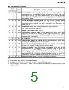
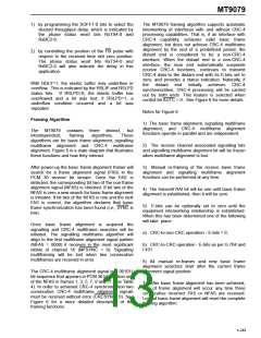
MT9079
don't care, CAR data D7 - D0 = page number).
Second, each page has a maximum of 16 registers
that are addressed on a read or write to a non-CAR
address (non-CAR: address AC4 = 1, AC3-AC0 =
register address, D7-D0 = data). Once a page of
memory is selected, it is only necessary to write to
the CAR when a different page is to be accessed.
See Figure 17 for timing requirements.
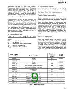
b) Page address or data byte -
D7 D6 D5 D4 D3
D2
D1
D0
See Figures 18 and 19 for timing requirements.
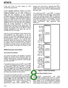
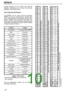
Register Access and Locations
Table 2 associates the MT9079 control and status
pages with access and page descriptions, as well as
an ST-BUS stream. When ST-BUS access mode is
used, each page contains 16 registers that are
associated consecutively with the first or second 16
channels of each ST-BUS stream. That is, page 1
register locations 10000 to 11111 appear on CSTi0
time slots 0 to 15, and page 2 register locations
10000 to 11111 appear on CSTi0 time slots 16 to 31.
It should be noted that access to the transmit and
receive circular buffers is not supported in ST-BUS
mode.
Communications between a serial controller and
MT9079 is
a
two byte operations. First,
a
Command/Address byte selects the address and
operation that follows. That is, the R/W bit selects a
read or write function and A determines if the next
4
byte is a new memory page address (A = 0) or a
4
data transfer within the current memory page (A =
4
1). The second byte is either a new memory page
address (when A = 0) or a data byte (when A = 1).
4
4
This is illustrated as follows:
a) Command/Address byte -
Common ST-BUS Streams
R/W
X
X
A
A
A
A
A
0
4
3
2
1
There are several control and status ST-BUS
streams that are common to all modes. CSTo1
contains the received channel associated signalling
bits (e.g., CCITT R1 and R2 signalling), and when
control bit RPSIG = 0, CSTi2 is used to control the
transmit channel associated signalling. DSTi and
DSTo contain the transmit and receive voice and
digital data. Figures 4a, b and c illustrate the relative
where:
R/W
X
- read or write operation,
- no function,
A = 0 - new memory page address to follow,
4
A = 1 - data byte to follow, and
4
A -A - determines the byte address.
3
0
Processor/
ST-BUS
Page Address
D7 - D0
Register Description
Controller
Access
Access
00000001
00000010
00000011
00000100
00000101
00000110
00000111
00001000
00001001
00001010
00001011
00001100
00001101
00001110
Master
Control
R/W
R/W
R
CSTi0
Master
Status
CSTo0
R/W
R/W
R
Per Channel Transmit Signalling
Per Channel Receive Signalling
CSTi2
CSTo1
CSTi1
Per Time Slot
Control
R/W
R/W
R/W
R/W
R
Transmit Circular Buffer Zero
Transmit Circular Buffer One
Receive Circular Buffer Zero
Receive Circular Buffer One
Transmit National Bit Buffer
Receive National Bit Buffer
---
---
---
---
---
---
R
R/W
R
Table 2 - Register Summary
4-245

 MITEL [ MITEL NETWORKS CORPORATION ]