MT9079
Pin Description (Continued)
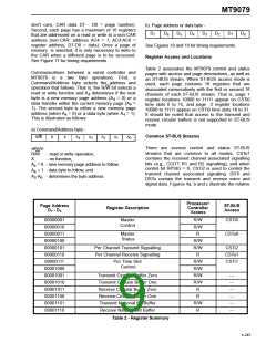
Pin #
Name
Description (see notes 1, 2 and 3)
DIP PLCC QFP
31 34 28
RxMF Receive Multiframe Boundary (Output): An output pulse delimiting the received
multiframe boundary. The next frame output on the data stream (DSTo) is basic frame
zero on the PCM 30 link. This receive multiframe signal can be related to either the
receive CRC multiframe (MFSEL=1) or the receive signalling multiframe (MFSEL=0).
See Figures 25 and 26.
32 35 29
TxMF Transmit Multiframe Boundary (Input): This input is used to set the channel
associated and CRC transmit multiframe boundary. The device will generate its own
multiframe if this pin is held high. This input is pulled high in most applications. See
Figures 24 to 26.
33 36 30
S/P
Serial/Parallel (Input): High - serial controller port or ST-BUS operation.
Low - parallel processor port operation.
34 37 31
35 38 32
VSS
Negative Power Supply (Input): Ground.
CSTi2 Control ST-BUS Input Two (Input): A 2.048 Mbit/s ST-BUS control stream which
contains the 30 (ABCDXXXX) transmit signalling nibbles when RPSIG=0. When
RPSIG=1 this pin has no function. Only the most significant nibbles of each ST-BUS
timeslot are valid. See Figure 4c.
-
39 33
NC
No Connection.
36 40 34 CSTo1 Control ST-BUS Output One (Output): A 2.048 Mbit/s serial status stream which
provides the 30 (ABCDXXXX) receive signalling nibbles.
37 41 35
38 42 36
TAIS Transmit Alarm Indication Signal (Input): High - TxA and TxB will transmit data
normally. Low - TxA and TxB transmits an AIS (all ones signal).
TxB
TxA
IC
Transmit B (Output): A split phase unipolar signal suitable for use with TxA, an
external line driver and a transformer to construct a bipolar PCM 30 line signal. This
output can also transmit RZ and NRZ bipolar signals. See Figures 28 and 30.
39 43 37
Transmit A (Output):A split phase unipolar signal suitable for use with TxB, an
external line driver and a transformer to construct a bipolar PCM 30 line signal. This
output can also transmit RZ and NRZ bipolar signals. See Figures 28 and 30.
40 44 38
Notes:
Internal Connection (Input): Connect to ground for normal operation.
1. All inputs are CMOS with TTL compatible logic levels.
2. All outputs are CMOS and are compatible with both TTL and CMOS logic levels.
3. See AC Electrical Characteristics - Timing Parameter Measurement Voltage Levels for input and output
voltage thresholds.
4-241

 MITEL [ MITEL NETWORKS CORPORATION ]