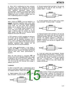
MT9079
TAIS Operation
modes, but cannot be accessed in ST-BUS mode. In
ST-BUS mode access to the national bits can be
achieved through the Transmit and Receive
Non-frame Alignment Signal (CSTi0 and CSTo).
When selected, the Data Link (DL) pin functions
override the transmit national bit buffer function.
The TAIS (Transmit AIS) pin allows the PRI interface
to transmit an all ones signal form the point of
power-up without writing to any control registers.
After the interface has been initialized normal
operation can take place by making TAIS high.
The CALN (CRC-4 Alignment) status bit and
maskable interrupt CALNI indicate the beginning of
every received CRC-4 multiframe.
National Bit Buffers
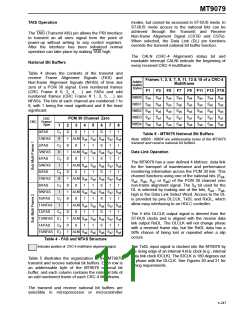
Table 4 shows the contents of the transmit and
receive Frame Alignment Signals (FAS) and
Non-frame Alignment Signals (NFAS) of time slot
zero of a PCM 30 signal. Even numbered frames
(CRC Frame # 0, 2, 4, ...) are FASs and odd
numbered frames (CRC Frame # 1, 3, 5, ...) are
NFASs. The bits of each channel are numbered 1 to
8, with 1 being the most significant and 8 the least
significant.
Frames 1, 3, 5, 7, 9, 11, 13 & 15 of a CRC-4
Addre
Multiframe
ssable
Bytes
F1 F3 F5 F7 F9 F11 F13 F15
NBB0
NBB1
NBB2
NBB3
NBB4
S
S
S
S
S
S
S
S
S
S
S
S
S
S
S
S
S
S
S
S
S
S
S
S
S
S
S
S
S
S
S
S
S
S
S
S
S
S
S
S
a4
a5
a6
a7
a8
a4
a5
a6
a7
a8
a4
a5
a6
a7
a8
a4
a5
a6
a7
a8
a4
a5
a6
a7
a8
a4
a5
a6
a7
a8
a4
a5
a6
a7
a8
a4
a5
a6
a7
a8
PCM 30 Channel Zero
CRC
Frame/
Type
CRC
1
2
0
1
0
1
0
1
0
1
0
1
0
1
0
1
0
1
3
4
5
6
7
8
0/FAS
C
0
1
1
0
1
1
1
Table 5 - MT9079 National Bit Buffers
Note: NBB0 - NBB4 are addressable bytes of the MT9079
transmit and receive national bit buffers.
1/NFAS
2/FAS
0
ALM S
S
S
S
S
a7 a8
a4
a4
a4
a4
a4
a4
a4
a4
a5
a6
C
0
1
1
0
1
1
2
3/NFAS
4/FAS
0
ALM S
S
S
S
S
a8
Data Link Operation
a5
a6
a7
C
0
1
1
0
1
1
3
The MT9079 has a user defined 4 kbit/sec. data link
for the transport of maintenance and performance
monitoring information across the PCM 30 link. This
5/NFAS
6/FAS
1
ALM S
S
S
S
S
a7 a8
a5
a6
C
0
1
1
0
1
1
4
channel functions using one of the national bits (S ,
a4
7/NFAS
8/FAS
0
ALM S
S
S
S
S
a7 a8
a5
a6
S , S , S or S ) of the PCM 30 channel zero
a5
a6
a7
a8
C
0
1
1
0
1
1
non-frame alignment signal. The S bit used for the
1
a
DL is selected by making one of the bits, S - S ,
a4
a8
9/NFAS
10/FAS
11/NFAS
12/FAS
13/NFAS
14/FAS
15/NFAS
1
ALM S
S
S
S
S
a7 a8
a5
a6
high in the Data Link Select Word. Access to the DL
is provided by pins DLCLK, TxDL and RxDL, which
allow easy interfacing to an HDLC controller.
C
0
1
1
0
1
1
2
1
ALM S
S
S
S
S
a7 a8
a5
a6
C
0
1
1
0
1
1
3
1
4
2
The 4 kHz DLCLK output signal is derived from the
ST-BUS clocks and is aligned with the receive data
link output RxDL. The DLCLK will not change phase
with a received frame slip, but the RxDL data has a
50% chance of being lost or repeated when a slip
occurs.
E
C
E
ALM S
S
S
S
S
a7 a8
a5
a6
0
1
1
0
1
1
ALM S
S
S
S
S
a7 a8
a5
a6
Table 4 - FAS and NFAS Structure
indicates position of CRC-4 multiframe alignment signal.
The TxDL input signal is clocked into the MT9079 by
the rising edge of an internal 4 kHz clock (e.g., internal
data link clock IDCLK). The IDCLK is 180 degrees out
of phase with the DLCLK. See Figures 20 and 21 for
timing requirements.
Table 5 illustrates the organization of the MT9079
transmit and receive national bit buffers. Each row is
an addressable byte of the MT9079 national bit
buffer, and each column contains the national bits of
an odd numbered frame of each CRC-4 Multiframe.
The transmit and receive national bit buffers are
selectible in microprocessor or microcontroller
4-247

 MITEL [ MITEL NETWORKS CORPORATION ]