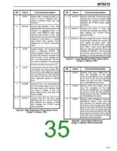
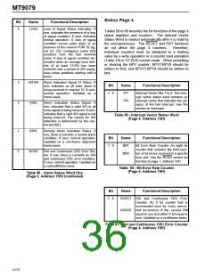
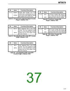
MT9079
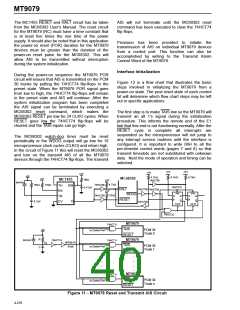
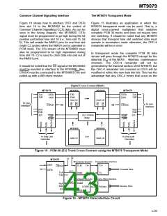
The data link transmit and receive signals are
connected directly to port one. The DCLK signal is
connected to INT1 so the 80C52 will be interrupted
when new data link data needs to be transported.
RD signals are re-timed using the CLKOUT signal to
generate a DS signal for the MT9079. The inverted
form of DT/R is used to make a R/W signal, and the
ALE is used to latch the lower order address lines for
the duration of the access cycle.
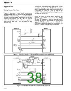
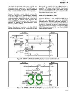
Figure 9 illustrates a circuit that will interface the
MT9079 to the MC68302 microprocessor operating
at 20 MHz. CS0 was chosen so that no external
address decoding would be required. The MT9079
does not have a DTACK output therefore, the
MC68302 DTACK should be tied high. The data link
interface is handled by Non-multiplexed Serial
Interface port Two (NMSI2).
MT9079 TAIS and Reset Circuit
Figure 11 illustrates a reset and transmit AIS circuit
that can be implemented with the MC68302
microprocessor. This circuit has three purposes: 1)
to provide a power-on reset for the all the MT9079
devices; 2) to have all the MT9079 devices transmit
AIS during system initialization; and 3) to have all the
MT9079 devices transmit AIS when the MC68302
watch-dog time expires.
Figure 10 shows how to connect a 16 MHz 80C188
microprocessor to the MT9079. The 80C188 WR and
MC68302
MT9079
EXTAL
XTAL
CS0
CS
+5V
10kΩ
25pF
25pF
700kΩ
4.7kΩ
10kΩ
10kΩ
+5V+5V
10kΩ
IRQ
DS
R/W
IRQ7
LDS
R/W
BERR
BGACK
AVEC
BR
5
8
+5V
A -A
AC -AC
0
4
7
0
4
D -D
D -D
0
0
7
+5V+5V
10kΩ
S/P
10kΩ
FRZ
BCLR
DTACK
RxD2
TxD2
RxDL
TxDL
DISCPU
BUSW
RCLK2
TCLK2
74HCT04
DLCLK
Figure 9 - MT9079 to MC68302 (20 MHz) Microprocessor Interface Circuit
80C188
MT9079
D -D
8
0
7
74F374
5
5
8
AD -AD
AC -AC
Dn
Qn
0
7
0
4
OE
CP
74F04
ALE
S/P
DS
74F74
74F86
74F04
RD
WR
CLKOUT
Q
D
Q
CLR
74F04
DT/R
R/W
CS
LCS, MCS,
UCS, or PCS
+5V
10kΩ
74F04
NMI
IRQ
Figure 10 - MT9079 to 80C188 (16 MHz) Microprocessor Interface Circuit
4-275

 MITEL [ MITEL NETWORKS CORPORATION ]