Preliminary Information
MT9076
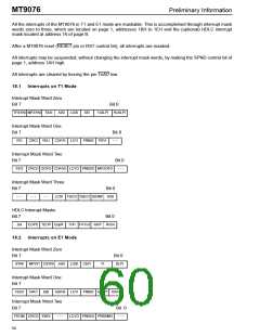
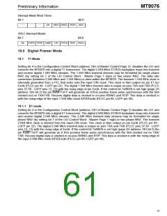
Interrupt Mask Word Three
Bit 7
Bit 0
- - -
- - -
- - -
JAI
1SECI 5SECI RCRI SIGI
HDLC Interrupt Masks
Bit 7
Bit 0
Ga
EOPD TEOP EopR TxFl FATxU RxFf RxOv
19.0 Digital Framer Mode
19.1
T1 Mode
Setting bit 4 in the Configuration Control Word (address 10H of Master Control Page 2) disables the LIU and
converts the MT9076 into a digital T1 transceiver. The digital 2.048 Mb/s ST-BUS backplane maps into transmit
and receive digital 1.544 Mb/s streams. The 1.544 Mb/s transmit streams may be formatted for single phase
NRZ (by setting bit 7 of the LIU Control Word - Master Page 1 high) or two phase NRZ. The data rate
conversion (between 2.048 Mb/s and 1.544 Mb/s) is done within the MT9076. The transmit 1.544 MHz clock is
internally generated from a PLL that locks onto the input C4b clock. This clock is then output on pin E1.5o/
Exclk (PLCC pin 44 - LQFP pin 22). The digital 1.544 Mb/s transmit data is output on pins TXA and TXB (PLCC
pins 37,38 - LQFP pins 12, 13) with the rising edge of pin Exclk. If the control bit Tx8KEN is set high (page 2H
address 10H bit 2) the pin RxMF/TxFP will generate an 8 KHz positive frame pulse synchronous with the Sbit
clocked out on TXA/TXB. Receive digital data is clocked in on pins RRING and RTIP. This data is clocked in
with the rising edge of the input 1.544 Mhz clock S/FR/Exclki (PLCC pin 66, LQFP pin 48).
19.1.1 E1 mode
Setting bit 4 in the Configuration Control Word (address 10H of Master Control Page 2) disables the LIU and
converts the MT9076 into a digital E1 transceiver. The digital 2.048 Mb/s ST-BUS backplane maps into transmit
and receive digital 2.048 Mb/s streams. The 2.048 Mb/s transmit data streams may be formatted for single
phase NRZ (by setting bit 7 of the LIU Control Word - Master Page 1 high) or two phase NRZ. The transmit
2.048 MHz clock is derived from the input C4b clock. This clock is then output on pin Exclk (PLCC pin 44 -
LQFP pin 22). The digital 2.048 Mb/s transmit data is output on pins TXA and TXB (PLCC pins 37,38 - LQFP
pins 12, 13) with the rising edge of Exclk. If the control bit Tx8KEN is set high (page 2H address 10H bit 2) the
pin RxMF/TxFP will generate an 8 KHz positive frame pulse synchronous with the Sbit clocked out on TXA/
TXB. Receive digital data is clocked in on pins RRING and RTIP. This data is clocked in with the rising edge of
the input 2.048 Mhz clock S/FR/Exclki (PLCC pin 66, LQFP pin 48).
57

 MITEL [ MITEL NETWORKS CORPORATION ]