MH89760B
Preliminary Information
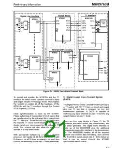
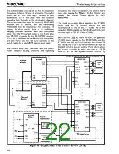
The switch matrix can be built so that the maximum
throughput delay is 1 frame +2 channels. The switch
matrix will not only route data channels to their
destination, but it will also route the received
signalling bits through to the destination channel.
This is necessary because the receiving MH89760B
decodes the T1 stream, and the transmitting
MH89760B has to reconstruct the outgoing T1
stream. In other words, there is no multiframe
integrity between received data and transmitted
data. The total throughput delay is one frame plus
ten ST-BUS channels for the MH89760B receiver,
2.5 ST-BUS channels for the MH89760B transmitter,
and one frame plus two ST-BUS channels for the
switch matrix for a total of 2.5 frames worst case.
through to the proper destination, the switch matrix
must also supply the Master Control Words, and
monitor the Master Status Words for each
MH89760B.
The clock generation block supplies the ST-BUS
clocks and the T1 transmit clocks that are
synchronized to one of the T1 trunks. All of the
extracted 8 kHz outputs are NANDed together before
they are input to PLL #2 of the MT8941.
Phase-locked Loop #2 of the MT8941, will generate
ST-BUS clock signals for the MH89760Bs and the
MT8980s that are synchronized with the chosen T1
line. The E8Ko of all of the other MH89760Bs can be
tristated from the Master Control Word, which allows
the system controller to select any one of 128 T1
lines to act as the synchronization source. By
The control block only interfaces with the switch
matrix. Besides routing channels and signalling
MH89760B
MT8980
Switch
Matrix
STo0
OUTA
DSTi
Equal-
izer
STi0
DSTo
OUTB
RxT
CSTi0
CSTo
CSTi1
RxR
STo7
STi7
F0i
C4i
C2i
F0i
E8Ko
C1.5i
MT8980
M
I
C
R
O
STo0
•
•
•
•
•
•
STi0
STo1
STo2
Control
Matrix
MH89760B
F0i
C4i
STo7
STi7
DSTi
OUTA
Equal-
izer
DSTo
CSTi0
CSTo
CSTi1
OUTB
RxT
MT8941
DPLL #1
RxR
Clock
Generator
C1.5i
F0i
CVb
F0i
C2i
12.352
MHz Osc.
C12i
F0i
E8Ko
C1.5i
DPLL #2
•
•
•
•
•
•
•
F0b
C8Kb
C16i
T1 Interfaces
C4i
C2i
C4b
C20
16.384
MHz Osc.
Figure 15 - Digital Access Cross Connect System (DACS)
4-76

 MITEL [ MITEL NETWORKS CORPORATION ]