MH89760B
Preliminary Information
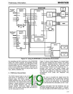
T1 Interface
Switch Matrix
Analog Line Interface
MH89760B
MT8980
PCMi
SLIC #1
STo0
T
DSTi
OUTA
•
STo1
STi1
•
PCMo
Equal-
izer
STi0
STo3
STi3
DSTo
CSTi0
CSTo
•
•
OUTB
RxT
CTLi
OFHK
STo2
STi2
•
R
•
•
•
STo4
CSTi1
•
•
•
•
MUX
RxR
•
•
•
•
C2i
F0i
C4i
F0i
SLIC #24
T
C1.5i
E8Ko
CTLo
R
OFHK
µP
MT8941
DPLL#1
Signalling Interface
CVb
F0i
C1.5i
12.352
C12i
PCMi
MHz Osc.
MT8964
MT8870
STD
Shift
Reg.
DPLL#2
•
#1
#1
F0i
F0b
•
C8Kb
C16i
D3
Do
C4i
C2i
C4b
C2o
16.384
MHz Osc.
•
•
•
•
•
•
MT8964
MT8870
STD
Shift
Reg.
#N
#N
D3
Do
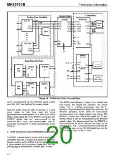
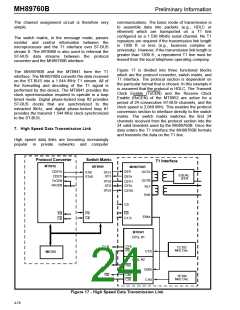
Figure 13 - PCM/Voice Data Channel Bank
easily accomplished by the MT8980 switch matrix
once the SLIC has digitized the analog signal.
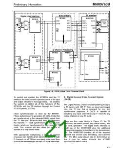
The ISDN channel bank in Figure 14 is divided into
four blocks, the digital line interface, the switch
matrix, the D channel processing, and the T1
interface. Beginning with the digital line interface, the
MT8910 provides 2B+D 160k bit bidirectional
communication over single twisted pair wiring. The
MT8910 converts the 160kbit line signal into ST-Bus
format, where it can be manipulated by the MT8980
switch matrix. The data received from the MT8910 is
then transferred to the D channel processor by the
switch matrix. The D channel processor converts the
2B+D format used on the 160 kBit digital line into the
23B+D format used on the T1 Link.
Channel banks must be able to operate in a loop
timed mode so that they meet the clock
synchronization requirements of a level four entity.
Phase-locked loop #2 of the MT8941 generates the
ST-BUS clocks that are synchronized to the
extracted 8kHz clock, and phase-locked loop #1
generates the transmit T1 clock synchronized to the
ST-BUS.
4. ISDN Voice/Data Channel Bank/Concentrator
The ISDN channel bank is a term that is used in this
context to describe a system that performs the same
logical function as the D3/D4 channel bank. That is,
it concentrates the subscribers digital loop into the
primary digital transmission scheme, the T1 trunk.
4-74

 MITEL [ MITEL NETWORKS CORPORATION ]