ProASIC3 DC and Switching Characteristics
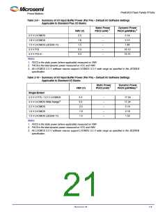
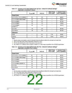
Table 2-11 • Summary of I/O Output Buffer Power (per pin) – Default I/O Software Settings1
Applicable to Advanced I/O Banks
Static Power
PDC3 (mW)2
Dynamic Power
CLOAD (pF)
VCCI (V)
PAC10 (µW/MHz)3
Single-Ended
3.3 V LVTTL / 3.3 V LVCMOS
3.3 V LVCMOS Wide Range4
2.5 V LVCMOS
35
35
35
35
35
3.3
3.3
2.5
1.8
1.5
–
–
–
–
–
468.67
468.67
267.48
149.46
103.12
1.8 V LVCMOS
1.5 V LVCMOS
(JESD8-11)
3.3 V PCI
3.3 V PCI-X
Differential
LVDS
10
10
3.3
3.3
–
–
201.02
201.02
–
–
2.5
3.3
7.74
88.92
LVPECL
Notes:
19.54
166.52
1. Dynamic power consumption is given for standard load and software default drive strength and output slew.
2. PDC3 is the static power (where applicable) measured on VCCI.
3. PAC10 is the total dynamic power measured on VCC and VCCI.
4. All LVCMOS 3.3 V software macros support LVCMOS 3.3 V wide range as specified in the JESD8-B specification.
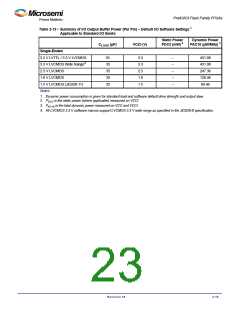
Table 2-12 • Summary of I/O Output Buffer Power (Per Pin) – Default I/O Software Settings1
Applicable to Standard Plus I/O Banks
Static Power
PDC3 (mW)2
Dynamic Power
CLOAD (pF)
VCCI (V)
PAC10 (µW/MHz)3
Single-Ended
3.3 V LVTTL / 3.3 V LVCMOS
3.3 V LVCMOS Wide Range4
2.5 V LVCMOS
35
35
35
35
35
10
10
3.3
3.3
2.5
1.8
1.5
3.3
3.3
–
–
–
–
–
–
–
452.67
452.67
258.32
133.59
92.84
1.8 V LVCMOS
1.5 V LVCMOS (JESD8-11)
3.3 V PCI
184.92
184.92
3.3 V PCI-X
Notes:
1. Dynamic power consumption is given for standard load and software default drive strength and output slew.
2.
P
is the static power (where applicable) measured on VMV.
DC3
3.
P
is the total dynamic power measured on VCC and VMV.
AC10
4. All LVCMOS 3.3 V software macros support LVCMOS 3.3 V wide range as specified in the JESD8-B specification.
2-9
Revision 18

 MICROSEMI [ Microsemi ]