ProASIC3 Flash Family FPGAs
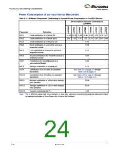
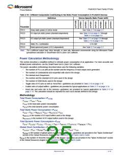
Table 2-15 • Different Components Contributing to the Static Power Consumption in ProASIC3 Devices
Definition
Device Specific Static Power (mW)
Parameter
PDC1
Array static power in Active mode
See Table 2-7 on page 2-7.
PDC2
I/O input pin static power (standard-dependent)
See Table 2-8 on page 2-7 through
Table 2-10 on page 2-8.
PDC3
I/O output pin static power (standard-dependent)
See Table 2-11 on page 2-9 through
Table 2-13 on page 2-10.
PDC4
PDC5
Static PLL contribution
2.55 mW
Bank quiescent power (VCCI-dependent)
See Table 2-7 on page 2-7.
Note: *For a different output load, drive strength, or slew rate, Microsemi recommends using the Microsemi Power
spreadsheet calculator or SmartPower tool in Libero SoC software.
Power Calculation Methodology
This section describes a simplified method to estimate power consumption of an application. For more accurate and
detailed power estimations, use the SmartPower tool in Libero SoC software.
The power calculation methodology described below uses the following variables:
•
•
•
•
•
•
•
•
The number of PLLs as well as the number and the frequency of each output clock generated
The number of combinatorial and sequential cells used in the design
The internal clock frequencies
The number and the standard of I/O pins used in the design
The number of RAM blocks used in the design
Toggle rates of I/O pins as well as VersaTiles—guidelines are provided in Table 2-16 on page 2-14.
Enable rates of output buffers—guidelines are provided for typical applications in Table 2-17 on page 2-14.
Read rate and write rate to the memory—guidelines are provided for typical applications in Table 2-17 on
page 2-14. The calculation should be repeated for each clock domain defined in the design.
Methodology
Total Power Consumption—P
TOTAL
PTOTAL = PSTAT + PDYN
PSTAT is the total static power consumption.
PDYN is the total dynamic power consumption.
Total Static Power Consumption—P
STAT
PSTAT = PDC1 + NINPUTS* PDC2 + NOUTPUTS* PDC3
NINPUTS is the number of I/O input buffers used in the design.
NOUTPUTS is the number of I/O output buffers used in the design.
Total Dynamic Power Consumption—P
DYN
PDYN = PCLOCK + PS-CELL + PC-CELL + PNET + PINPUTS + POUTPUTS + PMEMORY + PPLL
Global Clock Contribution—P
CLOCK
PCLOCK = (PAC1 + NSPINE*PAC2 + NROW*PAC3 + NS-CELL* PAC4) * FCLK
NSPINE is the number of global spines used in the user design—guidelines are provided in the "Spine Architecture"
section of the Global Resources chapter in the ProASIC3 FPGA Fabric User's Guide.
NROW is the number of VersaTile rows used in the design—guidelines are provided in the "Spine Architecture" section
of the Global Resources chapter in the ProASIC3 FPGA Fabric User's Guide.
Revision 18
2-12

 MICROSEMI [ Microsemi ]