ProASIC3 DC and Switching Characteristics
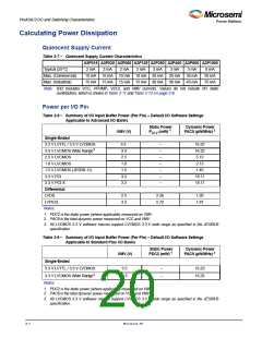
Calculating Power Dissipation
Quiescent Supply Current
Table 2-7 • Quiescent Supply Current Characteristics
A3P015 A3P030 A3P060 A3P125 A3P250 A3P400 A3P600 A3P1000
Typical (25°C)
2 mA
2 mA
2 mA
2 mA
3 mA
3 mA
20 mA
30 mA
5 mA
30 mA
45 mA
8 mA
50 mA
75 mA
Max. (Commercial)
Max. (Industrial)
10 mA 10 mA 10 mA 10 mA 20 mA
15 mA 15 mA 15 mA 15 mA 30 mA
Note: IDD Includes VCC, VPUMP, VCCI, and VMV currents. Values do not include I/O static
contribution, which is shown in Table 2-11 and Table 2-12 on page 2-9.
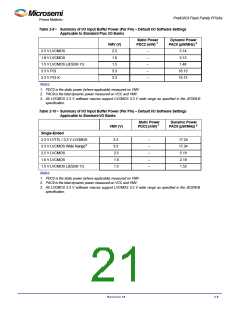
Power per I/O Pin
Table 2-8 • Summary of I/O Input Buffer Power (Per Pin) – Default I/O Software Settings
Applicable to Advanced I/O Banks
Static Power
PDC2 (mW) 1
Dynamic Power
PAC9 (µW/MHz) 2
VMV (V)
Single-Ended
3.3 V LVTTL / 3.3 V LVCMOS
3.3 V LVCMOS Wide Range3
2.5 V LVCMOS
1.8 V LVCMOS
1.5 V LVCMOS (JESD8-11)
3.3 V PCI
3.3
3.3
2.5
1.8
1.5
3.3
3.3
–
–
–
–
–
–
–
16.22
16.22
5.12
2.13
1.45
18.11
18.11
3.3 V PCI-X
Differential
LVDS
2.5
3.3
2.26
5.72
1.20
1.87
LVPECL
Notes:
1. PDC2 is the static power (where applicable) measured on VMV.
2. PAC9 is the total dynamic power measured on VCC and VMV.
3. All LVCMOS 3.3 V software macros support LVCMOS 3.3 V wide range as specified in the JESD8-B
specification.
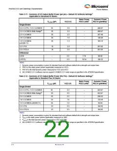
Table 2-9 • Summary of I/O Input Buffer Power (Per Pin) – Default I/O Software Settings
Applicable to Standard Plus I/O Banks
Static Power
PDC2 (mW) 1
Dynamic Power
PAC9 (µW/MHz) 2
VMV (V)
Single-Ended
3.3 V LVTTL / 3.3 V LVCMOS
3.3 V LVCMOS Wide Range3
Notes:
3.3
3.3
–
–
16.23
16.23
1. PDC2 is the static power (where applicable) measured on VMV.
2. PAC9 is the total dynamic power measured on VCC and VMV.
3. All LVCMOS 3.3 V software macros support LVCMOS 3.3 V wide range as specified in the JESD8-B
specification.
2-7
Revision 18

 MICROSEMI [ Microsemi ]