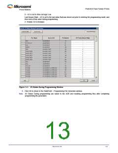
ProASIC3 Flash Family FPGAs
I/O Power-Up and Supply Voltage Thresholds for Power-On Reset
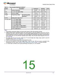
(Commercial and Industrial)
Sophisticated power-up management circuitry is designed into every ProASIC®3 device. These circuits ensure easy
transition from the powered-off state to the powered-up state of the device. The many different supplies can power up
in any sequence with minimized current spikes or surges.
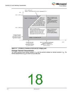
In addition, the I/O will be in a known state through the power-up sequence. The basic principle is shown in Figure 2-2
on page 2-5.
There are five regions to consider during power-up.
ProASIC3 I/Os are activated only if ALL of the following three conditions are met:
1. VCC and VCCI are above the minimum specified trip points (Figure 2-2 on page 2-5).
2. VCCI > VCC – 0.75 V (typical)
3. Chip is in the operating mode.
VCCI Trip Point:
Ramping up: 0.6 V < trip_point_up < 1.2 V
Ramping down: 0.5 V < trip_point_down < 1.1 V
VCC Trip Point:
Ramping up: 0.6 V < trip_point_up < 1.1 V
Ramping down: 0.5 V < trip_point_down < 1 V
VCC and VCCI ramp-up trip points are about 100 mV higher than ramp-down trip points. This specifically built-in
hysteresis prevents undesirable power-up oscillations and current surges. Note the following:
•
•
During programming, I/Os become tristated and weakly pulled up to VCCI.
JTAG supply, PLL power supplies, and charge pump VPUMP supply have no influence on I/O behavior.
PLL Behavior at Brownout Condition
Microsemi recommends using monotonic power supplies or voltage regulators to ensure proper power-up behavior.
Power ramp-up should be monotonic at least until VCC and VCCPLLX exceed brownout activation levels. The VCC
activation level is specified as 1.1 V worst-case (see Figure 2-2 on page 2-5 for more details).
When PLL power supply voltage and/or VCC levels drop below the VCC brownout levels (0.75 V ± 0.25 V), the PLL
output lock signal goes low and/or the output clock is lost. Refer to the "Power-Up/Down Behavior of Low Power Flash
Devices" chapter of the ProASIC3 FPGA Fabric User’s Guide for information on clock and lock recovery.
Internal Power-Up Activation Sequence
1. Core
2. Input buffers
Output buffers, after 200 ns delay from input buffer activation.
Thermal Characteristics
Introduction
The temperature variable in the Microsemi Designer software refers to the junction temperature, not the ambient
temperature. This is an important distinction because dynamic and static power consumption cause the chip junction
to be higher than the ambient temperature.
EQ can be used to calculate junction temperature.
TJ = Junction Temperature = T + TA
where:
TA = Ambient Temperature
T = Temperature gradient between junction (silicon) and ambient T = ja * P
ja = Junction-to-ambient of the package. ja numbers are located in Table 2-5 on page 2-6.
P = Power dissipation
Revision 18
2-4

 MICROSEMI [ Microsemi ]