SDA 9380 - B21
Preliminary Data Sheet
Recommended operating conditions
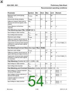
Parameter
Symbol Min
Nom Max
Unit Remark
Maximum input current during
clamping
I
100
µA
i-clamp
Internal bias during clamping
V
0.6
V
clamp
Difference between black level of
internal and external signals at the
outputs
∆V
50
mV
o
Delay difference of the three
channels
∆t
0
ns
1)
d
Fast Blanking Input FBL1 (RGB/YUV 1)
Input voltage no data insertion
Input voltage data insertion
Maximum input voltage
V
V
V
0.5
V
i-n
0.9
V
i-y
3.3
10
V
i-max
Difference between transit times for t - t
ns
1)
s
i
signal switching and signal insertion
Suppression of internal video signals
(insertion) or external video signals
(no insertion)
55
dB
f = 0 to 10 MHz, 1)
i
Fast Blanking/Contrast Reduction Input FBL2 (RGB2)
Maximum input voltage
V
3.3
10
V
i-max
Difference between transit times for t - t
ns
1)
s
i
signal switching and signal insertion
Suppression of internal video signals
(insertion) or external video signals
(no insertion)
55
dB
f = 0 to 10 MHz, 1)
i
Fast Blanking (Control bit COR1..COR0 = 00)
Input voltage no data insertion
Input voltage data insertion
V
0.5
V
V
i-n
i-y
V
0.9
Fast Blanking and Contrast Reduction (Control bit COR1..COR0 = 01...11)
Input voltage no contrast reduction
of internal RGB signals
V
1.4
0.5
V
V
%
V
FBL2L = 0
FBL2L = 1
icr-n
Input voltage contrast reduction of
internal RGB signals
V
1.7
0.9
FBL2L = 0
FBL2L = 1
icr-y
Contrast reduction (control bit
COR1..COR0)
0
75
Input voltage no data insertion
V
2
1.2
FBL2L = 0
FBL2L = 1
i-n
Micronas
8-46
2001-01-29

 MICRONAS [ MICRONAS ]