SDA 9380 - B21
Preliminary Data Sheet
Recommended operating conditions
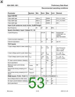
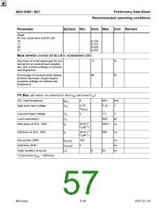
Parameter
Symbol Min
Nom Max
Unit Remark
Input VSYNC
Pulse width high
Pulse width high
Pulse width high
100 ns
100/fH
100/fH
100/fH
FH1_2=1, NI=0
200 ns
1.5/fH
FH1_2=0, NI=0
NI=1
Input CLKI (external clock mode, CLEXT=high)
Input frequency
25
27
30
MHz
MHz
Quartz Oscillator Input / Output X1, X2
Crystal frequency
24.576
fundamental
crystal type, e.g.
Saronix
9922 520 00282
Crystal resonant impedance
External capacitance
YUV Inputs
40
Ω
15
pF
see 10
Y input voltage (black-to-white value) V
1
0.7
1.5
1.05
V
V
P-P
only Y0 input at
YLL = 1, or at
HDTV matrix
U input voltage (peak-to-peak value) V
V input voltage (peak-to-peak value) V
1.33
0.7
2
1.05
V
V
U = - (B - Y),
at HDTV matrix
P-P
P-P
1.05
0.7
1.6
1.05
V
V
V = - (R - Y),
at HDTV matrix
DC input current between clamping
Input capacitance
I
100
7
nA
pF
µA
i
C
i
Maximum input current during
clamping
I
100
i-clamp
Internal bias during clamping at Y-
input
V
0.6
1.1
V
V
clampY
Internal bias during clamping at UV- V
inputs
clampUV
RGB Inputs (RGB2, RGB/YUV1 if RGBEN1=1, YUV/RGB0 if RGBEN0=1)
Input voltage (black-to-white value)
DC input current between clamping
Input capacitance
V
0.7
1
V
P-P
I
100
7
nA
pF
i
C
i
Micronas
8-45
2001-01-29

 MICRONAS [ MICRONAS ]