SDA 9380 - B21
Preliminary Data Sheet
Absolute maximum ratings
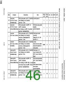
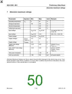
7 Absolute maximum ratings
Parameter
Symbol Min
Max
Unit Remark
Operating temperature
Storage temperature
Junction temperature
Soldering temperature
Input voltage
TA
0
70
°C
°C
°C
°C
-40
125
125
260
V
SS-0.3V
VDD+0.3V
not valid for SDA, SCL,
CLKI, HD
Input voltage
V
V
SS-0.3V
SS-0.3V
5.5V
SDA, SCL, CLKI, HD
Output voltage
Supply voltages
VDD+0.3V
3.8
VDD(D)
VDD(A1..4)
-0.3
V
V
Supply voltage
VDD(MC)
-0.3
9
Supply total voltage
difference
-0.25
0.25
V
between VDD(D),
VDD(A1..4)
VSS, SUBST total voltage
difference
-0.25
0.25
V
between SUBST,
VSS(MC), VSS(D),
VSS(A1..4)
Total power dissipation
Latch-up protection
1.28
100
W
-100
mA
all inputs/outputs
Absolute Maximum Ratings are those values beyond which damage to the device may occur. Func-
tional operation under these conditions or at any other condition beyond those indicated in the oper-
ational sections of this specification is not implied.
Micronas
7-42
2001-01-29

 MICRONAS [ MICRONAS ]