‡
Pre lim in a ry
MT9V012 - 1/6-In ch VGA CMOS Dig it a l Im a g e Se n so r
Fe a t u re De scrip t io n
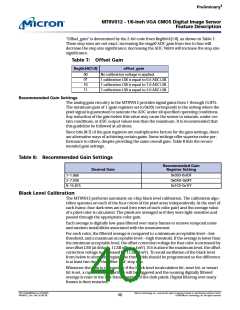
“Offset_gain” is determined by the 2-bit code from Reg0x5A[1:0], as shown in Table 7.
These step sizes are not exact; increasing the stage0 ADC gain from two to four will
decrease the step size significance; decreasing the ADC VREFD will increase the step size
significance.
Ta b le 7: Offse t Ga in
Re g 0x5A[1:0]
o ffse t _g a in
00
01
10
11
No calibration voltage is applied.
1 calibration LSB is equal to 0.5 ADC LSB.
1 calibration LSB is equal to 1.0 ADC LSB.
1 calibration LSB is equal to 2.0 ADC LSB.
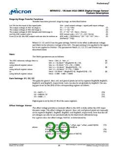
Re co m m e n d e d Ga in Se t t in g s
The analog gain circuitry in the MT9V012 provides signal gains from 1 through 15.875.
The minimum gain of 1 (gain registers set to 0x20) corresponds to the setting where the
pixel signal is guaranteed to saturate the ADC under all specified operating conditions.
Any reduction of the gain below this value may cause the sensor to saturate, under cer-
tain conditions, at ADC output values less than the maximum. It is recommended that
this guideline be followed at all times.
Since bits [8:7] of the gain registers are multiplicative factors for the gain settings, there
are alternative ways of achieving certain gains. Some settings offer superior noise per-
formance to others, despite providing the same overall gain. Table 8 lists the recom-
mended gain settings.
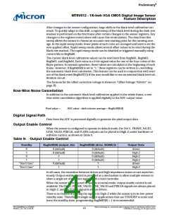
Ta b le 8: Re co m m e n d e d Ga in Se t t in g s
Re co m m e n d e d Ga in
Re g ist e r Se t t in g
De sire d Ga in
0x020–0x03F
0x0A0–0x0FF
0x1C0–0x1FF
1–1.969
2–7.938
8–15.875
Bla ck Le ve l Ca lib ra t io n
The MT9V012 performs automatic on-chip black level calibration. The calibration algo-
rithm operates on each of the four colors of the pixel array independently. At the start of
each frame, four dark rows are read (two rows of each color pair) and the average value
of a pixel color is calculated. The pixels are averaged as if they were light-sensitive and
passed through the appropriate color gain.
Each average is digitally low-pass filtered over many frames to remove temporal noise
and random instabilities associated with the measurement.
For each color, the filtered average is compared to a minimum acceptable level—low
threshold, and a maximum acceptable level—high threshold. If the average is lower than
the minimum acceptable level, the offset correction voltage for that color is increased by
one offset LSB (at default, 1 LSB offset = 1mV). If it is above the maximum level, the offset
correction voltage is decreased by 1 LSB (1mV). To avoid oscillation of the black level
from below to above the region, the thresholds should be programmed so the difference
is at least two times the offset DAC step size.
Whenever the gain is changed, or if the black level recalculation bit, reset bit, or restart
bit is set, a rapid sweep algorithm will be triggered and the running digitally filtered
average is reset to the first frame average of the dark pixels. Digital filtering over many
frames is then restarted.
PDF: 814eb99f/Source: 8175e929
MT9V012_2.fm - Rev. B 2/05 EN
Micron Technology, Inc., reserves the right to change products or specifications without notice.
40
©2004 Micron Technology, Inc. All rights reserved.

 MICRON [ MICRON TECHNOLOGY ]