‡
Pre lim in a ry
MT9V012 - 1/6-In ch VGA CMOS Dig it a l Im a g e Se n so r
Fe a t u re De scrip t io n
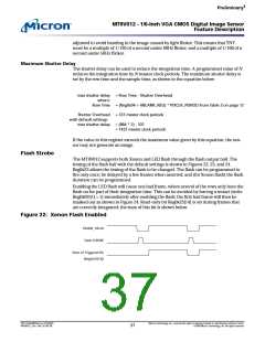
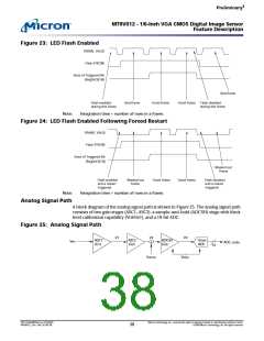
Fig u re 23: LED Fla sh En a b le d
FRAME_VALID
Flash STROBE
State of Triggered Bit
(Reg0x23[14])
Bad frame
Flash enabled
during this frame
Bad frame
Good frame
Good frame
Flash disabled
during this frame
Note:
Integration time = number of rows in a frame.
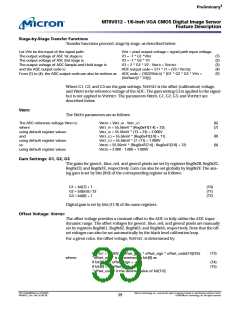
Fig u re 24: LED Fla sh En a b le d Fo llo w in g Fo rce d Re st a rt
FRAME_VALID
Flash STROBE
State of Triggered Bit
(Reg0x23[14])
Masked out
frame
Flash enabled
and a restart
triggered
Masked out
frame
Good frame
Good frame
Flash disabled
and a restart
triggered
Note:
Integration time = number of rows in a frame.
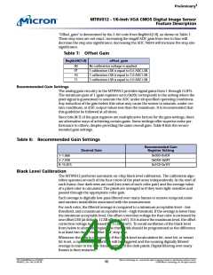
An a lo g Sig n a l Pa t h
A block diagram of the analog signal path is shown in Figure 25. The analog signal path
consists of two gain stages (ASC1, ASC2), a sample-and-hold (ADCSH) stage with black
level calibration capability (VOFFSET), and a 10-bit ADC.
Fig u re 25: An a lo g Sig n a l Pa t h
V1
V2
+
V3
ASC1
(G1)
ASC2
(G2)
ADCSH
(G3)
10-bit
ADC
VPIX
ADC_code
10
VOFFSET
VREFD
PDF: 814eb99f/Source: 8175e929
MT9V012_2.fm - Rev. B 2/05 EN
Micron Technology, Inc., reserves the right to change products or specifications without notice.
©2004 Micron Technology, Inc. All rights reserved.
38

 MICRON [ MICRON TECHNOLOGY ]