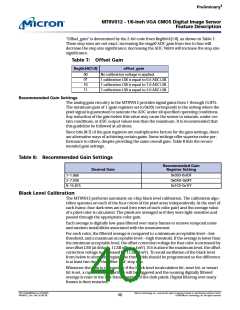
‡
Pre lim in a ry
MT9V012 - 1/6-In ch VGA CMOS Dig it a l Im a g e Se n so r
Fe a t u re De scrip t io n
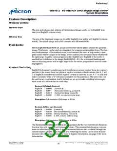
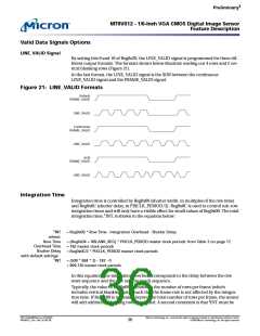
Va lid Da t a Sig n a ls Op t io n s
LINE_VALID Sig n a l
By setting bits 9 and 10 of Reg0x20, the LINE_VALID signal is programmed for three dif-
ferent output formats. The formats shown below illustrate reading out 4 rows and 2 ver-
tical blanking rows (Figure 21).
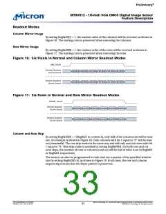
In the last format, the LINE_VALID signal is the XOR between the continuous
LINE_VALID signal and the FRAME_VALID signal.
Fig u re 21: LINE_VALID Fo rm a t s
Default
FRAME_VALID
LINE_VALID
Continuous
FRAME_VALID
LINE_VALID
XOR
FRAME_VALID
LINE_VALID
In t e g ra t io n Tim e
Integration time is controlled by Reg0x09 (shutter width, in multiples of the row time)
and Reg0x0C (shutter delay, in PIXCLK_PERIOD/ 2). Reg0x0C is used to control sub-row
integration times and will only have a visible effect for small values of Reg0x09. The total
t
integration time, INT, is shown in the equation below:
tINT
where:
=
Reg0x09 * Row Time - Integration Overhead - Shutter Delay
Row Time
=
=
=
(Reg0x04 + HBLANK_REG) * PIXCLK_PERIOD master clock periods from Table 3 on page 12
182 master clock periods
Reg0x0C/2 * PIXCLK_PERIOD master clock periods
Overhead Time
Shutter Delay
with default settings:
tINT
=
=
(509 * 884 * 2) - 182 - 0
899,730 master clock periods
In this equation, the integration overhead corresponds to the delay between the row
reset sequence and the row sample (read) sequence.
Typically, the value of Reg0x09 is limited to the number of rows per frame (which
includes vertical blanking rows), such that the frame rate is not affected by the integra-
tion time. If Reg0x09 is increased beyond the total number of rows per frame, the sensor
t
will add additional blanking rows as needed. A second constraint is that INT must be
PDF: 814eb99f/Source: 8175e929
MT9V012_2.fm - Rev. B 2/05 EN
Micron Technology, Inc., reserves the right to change products or specifications without notice.
36
©2004 Micron Technology, Inc. All rights reserved.

 MICRON [ MICRON TECHNOLOGY ]