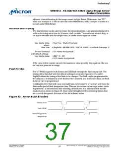
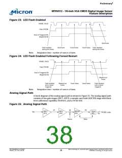
‡
Pre lim in a ry
MT9V012 - 1/6-In ch VGA CMOS Dig it a l Im a g e Se n so r
Fe a t u re De scrip t io n
After changes to the sensor configuration, large shifts in the black level calibration can
result. To quickly adapt to this shift, a rapid sweep of the black level during the dark-row
readout is performed on the first frame after certain changes to the sensor registers. Any
changes to the registers noted above will cause this recalculation. The data from this
sweep allows the sensor to choose an accurate new starting point for the running aver-
age. In the rapid sweep mode, fewer pixels of each color are averaged and used to set the
new applied offset. Rapid sweep mode allows several offset values to be tried during the
black row readout. The rapid sweep mode can be disabled or triggered manually using
control bits in Reg0x60.
The current black level calibration values can be read back from Reg0x61, Reg0x62,
Reg0x63, and Reg0x64. Each value is a 9-bit signed value for one of the four colors of the
Bayer pattern. In normal operation, these values are calculated at the beginning of each
frame. However, if Reg0x60[0] is set to “1,” these registers can be written to, overriding
the automatic black level calculation. This feature can be used in conjunction with read-
out of the black rows (Reg0x22[7]) if the user would like to use an external black level cal-
ibration circuit.
The formula for the offset correction voltage is shown in "Offset Voltage: VOFFSET" on
page 39.
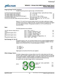
Ro w -Wise No ise Ca n ce lla t io n
In addition to the automatic black level calibration applied to the whole frame, a row-
wise noise cancellation algorithm is applied digitally to the ADC output value.
Pixel value =
ADC value - dark column average + Reg0x30[9:0]
Dig it a l Sig n a l Pa t h
Data from the ADC is processed digitally to generate the pixel output data.
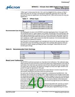
Ou t p u t En a b le Co n t ro l
When the sensor is configured to operate in default mode, the DOUT, FRAME_VALID,
LINE_VALID, PIXCLK, and FLASH outputs can be placed in High-Z under hardware or
software control, as shown in Table 9.
Ta b le 9: Ou t p u t En a b le Co n t ro l
St a n d b y
Re g 0x0D[4] (o u t p u t _d is)
Re g 0x0D[6] (d rive _SIGNALS)
Ou t p u t St a t e
0
0 (default)
0 (default)
0 (default)
0 (default)
0 (default)
1
driven
High-Z
High-Z
High-Z
driven
High-Z
1
0 (default)
0
1
1
1
“Don’t Care”
“Don’t Care”
0 (default)
1
1
In all cases, the transition between driven and high impedance states occurs asynchro-
nously. Output enable control is provided as a mechanism to allow multiple sensors to
share a single set of interface signals with a host controller.
When the sensor is configured to operate in serial mode, output enable control is not
available: The DOUT, FRAME_VALID, LINE_VALID and PIXCLK signals are always placed
in High-Z, and the FLASH signal is always driven.
There is no benefit in placing the signals in High-Z while the sensor is in its low-power
standby state. Therefore, in single-sensor applications that use STANDBY to enter and
leave the standby state, programming Reg0x0D[6] = 1 is recommended.
PDF: 814eb99f/Source: 8175e929
MT9V012_2.fm - Rev. B 2/05 EN
Micron Technology, Inc., reserves the right to change products or specifications without notice.
41
©2004 Micron Technology, Inc. All rights reserved.

 MICRON [ MICRON TECHNOLOGY ]