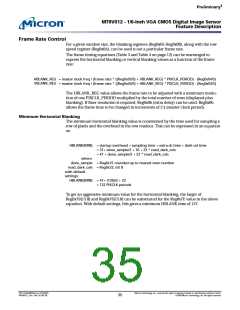
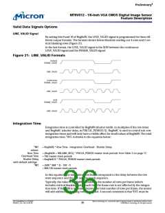
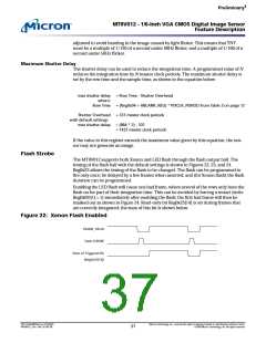
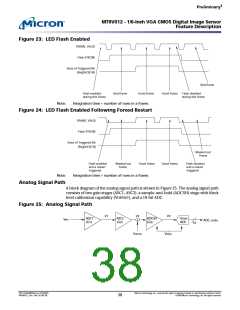
‡
Pre lim in a ry
MT9V012 - 1/6-In ch VGA CMOS Dig it a l Im a g e Se n so r
Fe a t u re De scrip t io n
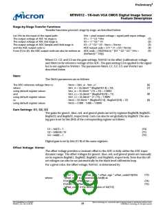
St a g e -b y-St a g e Tra n sfe r Fu n ct io n s
Transfer functions proceed, stage by stage, as described below:
Let VPIX be the input of the signal path:
The output voltage of ASC 1st stage is:
The output voltage of ASC 2nd stage is:
The output voltage of ADC Sample-and-Hold stage is:
and the ADC output code is:
VPIX = pixel output voltage = signal path input voltage,
V1 = -1 * G1 *VPIX
V2 = -1 * G2 * V1
V3 = 2 * G3 * V2 - VREFD + VOFFSET
ADC output code = 511 * (1 + (V3 / VrEFD))
(1)
(2)
(3)
(4)
(5)
From (1) to (4), the ADC output code can also be written as: ADC code = (1022/VREFD) * [G1 * G2 * G3 * VPIX +
(Voffset/(2 * G3))]
Where G1, G2, and G3 are the gain settings, VOFFSET is the offset (calibration) voltage,
and VREFD is the reference voltage of the ADC. The gain setting G3 is applied to the signal
but is not applied to VOFFSET. The parameters VREFD, G1, G2, G3, and VOFFSET are
described below.
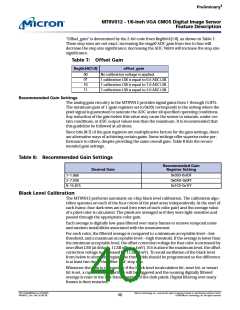
VREFD
The VREFD parameters are as follows:
(6)
(7)
The ADC reference voltage VREFD Is:
where
using default register values:
and
using default register values:
so
using default register values
VREFD = VREF_HI - VREF_LO
VREF_HI = 55.56mV * (Reg0x41[7:4] + 23)
VREF_HI = 55.56mV * (13 + 23) = 2.000V
VREF_LO = 55.56mV * (Reg0x41[3:0] + 11)
VREF_LO = 55.56mV * (7 +11) = 1.000V
VREFD = 55.56mV * (Reg0x41[7:4] - Reg0x41[3:0] + 12)
VREFD = 2.000 - 1.000 = 1.000V
(8)
(9)
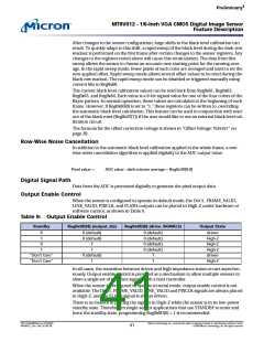
Ga in Se t t in g s: G1, G2, G3
The gains for green1, blue, red, and green2 pixels are set by registers Reg0x2B, Reg0x2C,
Reg0x2D, and Reg0x2E, respectively. Gain can also be set globally by Reg0x2F. The ana-
log gain is set by bits [8:0] of the corresponding register as follows:
(10)
(11)
(12)
G1 = bit[7] + 1
G2 = bit[6:0] / 32
G3 = bit[8] + 1
Digital gain is set by bits [11:9] of the same registers.
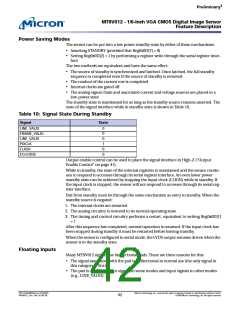
Offse t Vo lt a g e : VOFFSET
The offset voltage provides a constant offset to the ADC to fully utilize the ADC input
dynamic range. The offset voltages for green1, blue, red, and green2 pixels are manually
set by registers Reg0x61, Reg0x62, Reg0x63, and Reg0x64, respectively. Note that the off-
set voltages can also be set automatically by the black level calibration loop.
For a given color, the offset voltage, VOFFSET, is determined by:
(13)
VOFFSET = 0.250V * offset_gain * offset_sign * offset_code[7:0]/255
“offset_sign” is determined by bit[8] as:
if bit[8] = 0, offset_sign = +1
where:
(14)
(15)
if bit[8] = 1, offset_sign = -1
“offset_code” is the decimal value of bit[7:0]
PDF: 814eb99f/Source: 8175e929
MT9V012_2.fm - Rev. B 2/05 EN
Micron Technology, Inc., reserves the right to change products or specifications without notice.
©2004 Micron Technology, Inc. All rights reserved.
39

 MICRON [ MICRON TECHNOLOGY ]