‡
Pre lim in a ry
MT9V012 - 1/6-In ch VGA CMOS Dig it a l Im a g e Se n so r
Op e ra t in g Mo d e s
Op e ra t in g Mo d e s
The functional operating mode of the MT9V012 is controlled by the MODE1 and
MODE0 inputs (Table 2). These inputs should be driven to a static logic 1 or static logic 0
level during normal operation.
Ta b le 2: Fu n ct io n a l Mo d e Se le ct io n
Mo d e 1
Mo d e 0
De scrip t io n
Selects default mode
0
0
1
1
0
1
0
1
Selects serial mode
Not used
Not used
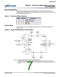
De fa u lt Mo d e
This section shows a typical configuration schematic for the MT9V012 operating in
default mode.
Fig u re 2: Typ ica l Co n fig u ra t io n : De fa u lt Mo d e
Analog
Power
Digital
Power
1
1
VDD
VAA
VAAPIX
MODE0
MODE1
CLKIN
MASTER CLOCK
(27 MHz)
DOUT(9
:0)
STANDBY
To
PIXCLK
From
Controller
Controller
LINE_VALID
FRAME_VALID
FLASH
S
DATA
SCLK
TEST
RESET#
10µF
DGND
AGND
Digital
Ground
Analog
Ground
Notes: 1. All power supplies should be adequately decoupled.
2. Resistor value 1.5KΩ is recommended, but may be greater for slower two-wire speed.
3. This pull-up resistor is not required if the controller drives a valid logic level on SCLK at all
times.
PDF: 814eb99f/Source: 8175e929
MT9V012_2.fm - Rev. B 2/05 EN
Micron Technology, Inc., reserves the right to change products or specifications without notice.
7
©2004 Micron Technology, Inc. All rights reserved.

 MICRON [ MICRON TECHNOLOGY ]