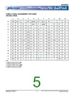
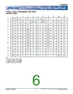
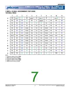
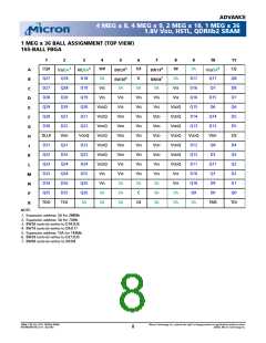
ADVANCE
4 MEG x 8, 4 MEG x 9, 2 MEG x 18, 1 MEG x 36
1.8V VDD, HSTL, QDRIIb2 SRAM
READ/WRITE OPERATIONS (continued)
PROGRAMMABLE IMPEDANCE OUTPUT
BUFFER
WRITE cycles are initiated by W# LOW at K rising
edge. The address for the WRITE cycle is provided at
the following K# rising edge. Data is expected at the
rising edge of K and K#, beginning at the same K that
initiated the cycle. Write registers are incorporated to
facilitate pipelined, self-timed WRITE cycles and to
provide fully coherent data for all combinations of
reads and writes. A read can immediately follow a
write, even if they are to the same address. Although
the write data has not been written to the memory
array, the SRAM will deliver the data from the write
register instead of using the older data from the mem-
ory array. The latest data is always utilized for all bus
transactions. WRITE cycles can be initiated on every K
rising edge.
The QDR SRAM is equipped with programmable
impedance output buffers. This allows a user to match
the driver impedance to the system. To adjust the
impedance, an external precision resistor (RQ) is con-
nected between the ZQ ball and VSS. The value of the
resistor must be five times the desired impedance. For
example, a 350ꢀ resistor is required for an output
impedance of 70ꢀ. To ensure that output impedance
is one-fifth the value of RQ (within 15 percent), the
range of RQ is 175ꢀ to 350ꢀ. Alternately, the ZQ ball
can be connected directly to VDDQ, which will place
the device in a minimum impedance mode.
Output impedance updates may be required
because variations may occur over time in supply volt-
age and temperature. The device samples the value of
RQ. Impedance updates are transparent to the system;
they do not affect device operation, and all data sheet
timing and current specifications are met during an
update.
The device will power up with an output impedance
set at 50ꢀ. To guarantee optimum output driver
impedance after power-up, the SRAM needs 1,024
cycles to update the impedance. The user can operate
the part with fewer than 1,024 clock cycles, but optimal
output impedance is not guaranteed.
PARTIAL WRITE OPERATIONS
BYTE WRITE operations are supported, except for
the x8 devices in which nibble write is supported. The
active LOW byte write controls, BWx# (NWx#), are reg-
istered coincident with their corresponding data. This
feature can eliminate the need for some READ-MOD-
IFY-WRITE cycles, collapsing it to a single BYTE/NIB-
BLE WRITE operation in some instances.
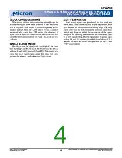
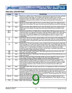
Figure 3
Application Example
SRAM #1
SRAM #4
B
R = 250Ω
R = 250Ω
Vt
ZQ
Q
C# K K#
ZQ
Q
C# K K#
B
R W W
# #
D
D
SA
R W W
# #
#
R
SA
C
#
C
DATA IN
DATA OUT
Address
Read#
Vt
Vt
R
BUS
MASTER
(CPU
Write#
BW#
or
ASIC)
Source K
Source K#
Delayed K
Delayed K#
R
R = 50Ω
Vt = VREF/2
NOTE:
In this approach, the second clock pair drives the C and C# clocks but is delayed such that return data meets data setup and
hold times at the bus master.
36Mb: 1.8V VDD, HSTL, QDRIIb2 SRAM
MT54W2MH18B_A.fm - Rev 9/02
Micron Technology, Inc., reserves the right to change products or specifications without notice.
©2002, Micron Technology Inc.
3

 MICRON [ MICRON TECHNOLOGY ]