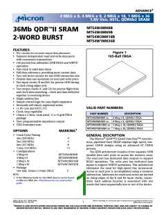
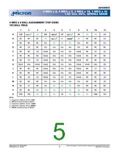
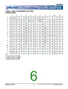
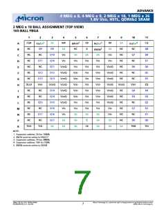
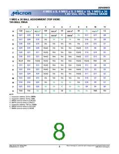
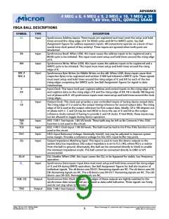
ADVANCE
4 MEG x 8, 4 MEG x 9, 2 MEG x 18, 1 MEG x 36
1.8V VDD, HSTL, QDRIIb2 SRAM
GENERAL DESCRIPTION (continued)
Since data can be transferred into and out of the
device on every rising edge of both clocks (K and K#, C
and C#), memory bandwidth is maximized while sys-
tem design is simplified by eliminating bus turn-
arounds.
The SRAM operates from a +1.8V power supply, and
all inputs and outputs are HSTL-compatible. The
device is ideally suited for applications that benefit
from a high-speed, fully-utilized DDR data bus.
Please refer to Micron’s Web site (www.micron.com/
sramds) for the latest data sheet.
Depth expansion is accomplished with port selects
for each port (read R#, write W#), which are received at
K rising edge. Port selects permit independent port
operation.
READ/WRITE OPERATIONS
All bus transactions operate on an uninterruptable
burst of two data, requiring one full clock cycle of bus
utilization. The resulting benefit is that short data
transactions can remain in operation on both buses
provided that the address rate can be maintained by
the system (2x the clock frequency).
All synchronous inputs pass through registers con-
trolled by the K or K# input clock rising edges. Active
LOW byte writes (BWx#) permit byte or nibble write
selection. Write data and byte writes are registered on
the rising edges of both K and K#. The addressing
within each burst of two is fixed and sequential, begin-
ning with the lowest and ending with the highest
address. All synchronous data outputs pass through
output registers controlled by the rising edges of the
output clocks (C and C# if provided, otherwise K and
K#).
Four balls are used to implement JTAG test capabili-
ties: test mode select (TMS), test data-in (TDI), test
clock (TCK), and test data-out (TDO). JTAG circuitry is
used to serially shift data to and from the SRAM. JTAG
inputs use JEDEC-standard 1.8V I/O levels to shift data
during this testing mode of operation.
READ cycles are pipelined. The request is initiated
by asserting R# LOW at K rising edge. Data is delivered
after the rising edge of K# (t + 1) using C and C# as the
output timing references or using K and K#, if C and C#
are tied HIGH. If C and C# are tied HIGH, they may not
be toggled during device operation. Output tri-stating
is automatically controlled such that the bus is
released if no data is being delivered. This permits
banked SRAM systems with no complex OE timing
generation. Back-to-back READ cycles are initiated
every K rising edge.
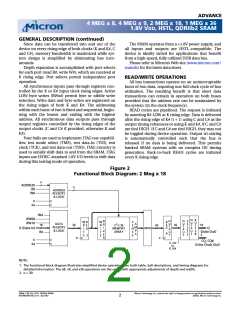
Figure 2
Functional Block Diagram: 2 Meg x 18
n
ADDRESS
R#
n
ADDRESS
REGISTRY
& LOGIC
W#
K
K#
W#
BW0#
BW1#
O
B
D
R
I
V
E
R
O
U
T
O
U
T
S
E
L
E
C
T
W R
R E
I G
T
W
R
I
T
E
S
E
N
S
R
E
U U
DATA
REGISTRY
& LOGIC
A
M
P
n
18
36
36
18
2
x 36
36
T
P
U
T
F
F
E
R
G
D (Data In)
MUX
Q
MEMORY
ARRAY
P
P
(Data Out)
2
R#
U
T
U
T
A
S
E 2
E
K
C
K
K#
CQ, CQ#
C, C#
(Echo Clock Out)
or
K, K#
NOTE:
1. The functional block diagram illustrates simplified device operation. See truth table, ball descriptions, and timing diagrams for
detailed information. The x8, x9, and x36 operations are the same, with apporpriate adjustments of depth and width.
2. n = 20
36Mb: 1.8V VDD, HSTL, QDRIIb2 SRAM
MT54W2MH18B_A.fm - Rev 9/02
Micron Technology, Inc., reserves the right to change products or specifications without notice.
©2002, Micron Technology Inc.
2

 MICRON [ MICRON TECHNOLOGY ]