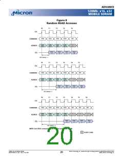
ADVANCE
128Mb: x16, x32
MOBILE SDRAM
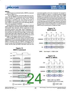
WRITEs
WRITE bursts are initiated with a WRITE command,
as shown in Figure 13.
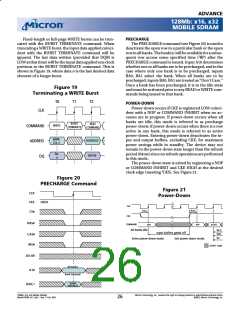
command applies to the new command. An example is
shown in Figure 15. Data n + 1 is either the last of a burst
of two or the last desired of a longer burst. The 128Mb
SDRAM uses a pipelined architecture and therefore does
not require the 2n rule associated with a prefetch archi-
tecture. A WRITE command can be initiated on any clock
cycle following a previous WRITE command. Full-speed
random write accesses within a page can be performed to
thesamebank, asshowninFigure16, oreachsubsequent
WRITE may be performed to a different bank.
The starting column and bank addresses are pro-
vided with the WRITE command, and auto precharge is
either enabled or disabled for that access. If auto
precharge is enabled, the row being accessed is
precharged at the completion of the burst. For the ge-
neric WRITE commands used in the following illustra-
tions, auto precharge is disabled.
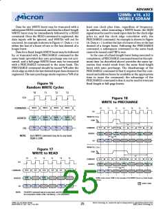
During WRITE bursts, the first valid data-in element
will be registered coincident with the WRITE command.
Subsequent data elements will be registered on each
successive positive clock edge. Upon completion of a
fixed-length burst, assuming no other commands have
been initiated, the DQs will remain High-Z and any addi-
tional input data will be ignored (see Figure 14). A full-
page burst will continue until terminated. (At the end of
the page, it will wrap to column 0 and continue.)
Data for any WRITE burst may be truncated with a
subsequentWRITEcommand, anddataforafixed-length
WRITE burst may be immediately followed by data for a
WRITE command. The new WRITE command can be
issued on any clock following the previous WRITE com-
mand, and the data provided coincident with the new
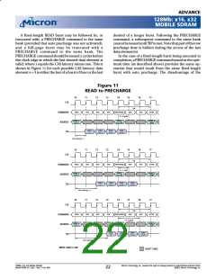
Figure 14
WRITE Burst
T0
T1
T2
T3
CLK
WRITE
NOP
NOP
NOP
COMMAND
ADDRESS
DQ
BANK,
COL n
DIN
DIN
n + 1
n
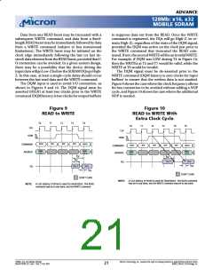
Figure 13
WRITE Command
NOTE:
Burst length = 2. DQM is LOW.
CLK
CKE HIGH
Figure 15
WRITE to WRITE
CS#
T0
T1
T2
RAS#
CLK
CAS#
WE#
WRITE
NOP
WRITE
COMMAND
ADDRESS
DQ
COLUMN
A0-A8
ADDRESS
BANK,
COL n
BANK,
COL b
A9, A11
DIN
DIN
DIN
b
ENABLE AUTO PRECHARGE
n
n + 1
A10
DISABLE AUTO PRECHARGE
NOTE:
DQM is LOW. Each WRITE
command may be to any bank.
BANK
ADDRESS
BA0,1
DON’T CARE
VALID ADDRESS
DON’T CARE
128Mb: x16, x32 Mobile SDRAM
MobileY95W_3V_F.p65 – Rev. F; Pub. 9/02
Micron Technology, Inc., reserves the right to change products or specifications without notice.
©2002, Micron Technology, Inc.
24

 MICRON [ MICRON TECHNOLOGY ]