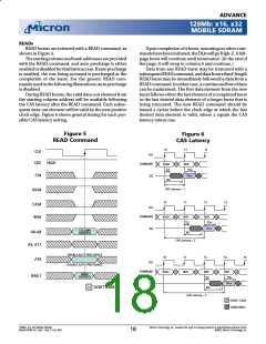
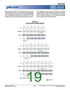
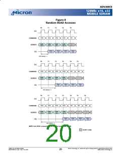
ADVANCE
128Mb: x16, x32
MOBILE SDRAM
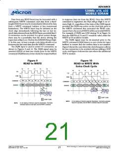
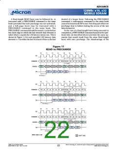
A fixed-length READ burst may be followed by, or
truncated with, a PRECHARGE command to the same
bank (provided that auto precharge was not activated),
and a full-page burst may be truncated with a
PRECHARGE command to the same bank. The
PRECHARGE command should be issued x cycles before
the clock edge at which the last desired data element is
valid, where x equals the CAS latency minus one. This is
shown in Figure 11 for each possible CAS latency; data
element n + 3 is either the last of a burst of four or the last
desired of a longer burst. Following the PRECHARGE
command, a subsequent command to the same bank
cannotbeissueduntil RPismet. Notethatpartoftherow
precharge time is hidden during the access of the last
data element(s).
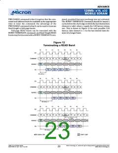
In the case of a fixed-length burst being executed to
completion, a PRECHARGE command issued at the opti-
mum time (as described above) provides the same op-
eration that would result from the same fixed-length
burst with auto precharge. The disadvantage of the
t
Figure 11
READ to PRECHARGE
T0
T1
T2
T3
T4
T5
T6
T7
CLK
t
RP
READ
NOP
NOP
NOP
PRECHARGE
NOP
NOP
ACTIVE
COMMAND
ADDRESS
DQ
X = 0 cycles
BANK
(a or all)
BANK a,
COL n
BANK a,
ROW
D
OUT
D
n + 1
OUT
DOUT
DOUT
n
n + 2
n + 3
CAS Latency = 1
T0
T1
T2
T3
T4
T5
T6
T7
CLK
t
RP
READ
NOP
NOP
NOP
PRECHARGE
NOP
NOP
ACTIVE
COMMAND
ADDRESS
DQ
X = 1 cycle
BANK
(a or all)
BANK a,
BANK a,
ROW
COL
n
D
OUT
D
n + 1
OUT
DOUT
DOUT
n + 3
n
n + 2
CAS Latency = 2
T0
T1
T2
T3
T4
T5
T6
T7
CLK
t
RP
READ
NOP
NOP
NOP
PRECHARGE
NOP
NOP
ACTIVE
COMMAND
ADDRESS
DQ
X = 2 cycles
BANK
(a or all)
BANK a,
BANK a,
ROW
COL
n
D
OUT
DOUT
DOUT
D
n + 3
OUT
n
n + 1
n + 2
CAS Latency = 3
NOTE: DQM is LOW.
DON’T CARE
128Mb: x16, x32 Mobile SDRAM
MobileY95W_3V_F.p65 – Rev. F; Pub. 9/02
Micron Technology, Inc., reserves the right to change products or specifications without notice.
©2002, Micron Technology, Inc.
22

 MICRON [ MICRON TECHNOLOGY ]