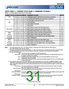
ADVANCE
128Mb: x16, x32
MOBILE SDRAM
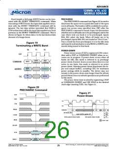
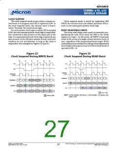
CLOCK SUSPEND
The clock suspend mode occurs when a column ac-
cess/burst is in progress and CKE is registered LOW. In
the clock suspend mode, the internal clock is deacti-
vated, “freezing” the synchronous logic.
Clock suspend mode is exited by registering CKE
HIGH; the internal clock and related operation will re-
sume on the subsequent positive clock edge.
For each positive clock edge on which CKE is sampled
LOW, the next internal positive clock edge is suspended.
Any command or data present on the input pins at the
time of a suspended internal clock edge is ignored; any
data present on the DQ pins remains driven; and burst
counters are not incremented, as long as the clock is
suspended. (See examples in Figures 22 and 23.)
BURST READ/SINGLE WRITE
The burst read/single write mode is entered by pro-
gramming the write burst mode bit (M9) in the mode
register to a logic 1. In this mode, all WRITE commands
result in the access of a single column location (burst of
one), regardless of the programmed burst length. READ
commandsaccesscolumnsaccordingtotheprogrammed
burst length and sequence, just as in the normal mode of
operation (M9 = 0).
Figure 22
Clock Suspend During WRITE Burst
Figure 23
Clock Suspend During READ Burst
T0
T1
T2
T3
T4
T5
T0
T1
T2
T3
T4
T5
T6
CLK
CKE
CLK
CKE
INTERNAL
CLOCK
INTERNAL
CLOCK
READ
NOP
NOP
NOP
NOP
NOP
COMMAND
ADDRESS
DQ
NOP
WRITE
NOP
NOP
COMMAND
ADDRESS
BANK,
COL n
BANK,
COL n
D
OUT
D
OUT
D
n + 2
OUT
DOUT
n + 3
n
n + 1
D
n
IN
D
n + 1
IN
DIN
n + 2
D
IN
DON’T CARE
NOTE: For this example, CAS latency = 2, burst length = 4 or greater, and
DON’T CARE
DQM is LOW.
128Mb: x16, x32 Mobile SDRAM
MobileY95W_3V_F.p65 – Rev. F; Pub. 9/02
Micron Technology, Inc., reserves the right to change products or specifications without notice.
©2002, Micron Technology, Inc.
27

 MICRON [ MICRON TECHNOLOGY ]