ADVANCE
128Mb: x16, x32
MOBILE SDRAM
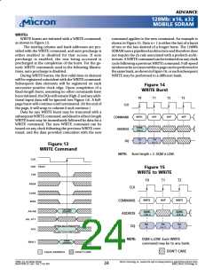
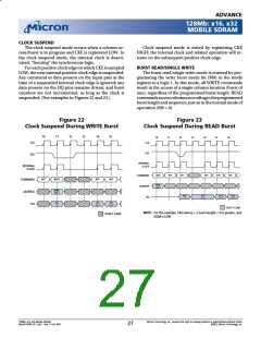
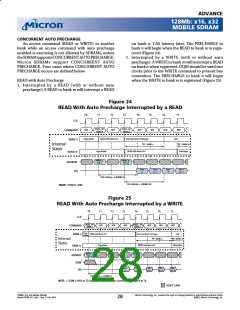
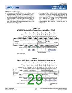
CONCURRENT AUTO PRECHARGE
An access command (READ or WRITE) to another
bank while an access command with auto precharge
enabled is executing is not allowed by SDRAMs, unless
theSDRAMsupportsCONCURRENTAUTOPRECHARGE.
Micron SDRAMs support CONCURRENT AUTO
PRECHARGE. Four cases where CONCURRENT AUTO
PRECHARGE occurs are defined below.
on bank n, CAS latency later. The PRECHARGE to
bank n will begin when the READ to bank m is regis-
tered (Figure 24).
2. Interrupted by a WRITE (with or without auto
precharge): A WRITE to bank m will interrupt a READ
on bank n when registered. DQM should be used two
clocks prior to the WRITE command to prevent bus
contention. The PRECHARGE to bank n will begin
when the WRITE to bank m is registered (Figure 25).
READ with Auto Precharge
1. Interrupted by a READ (with or without auto
precharge): A READ to bank m will interrupt a READ
Figure 24
READ With Auto Precharge Interrupted by a READ
T0
T1
T2
T3
T4
T5
T6
T7
CLK
READ - AP
BANK n
READ - AP
BANK m
NOP
NOP
NOP
NOP
NOP
NOP
COMMAND
Page Active
READ with Burst of 4
Interrupt Burst, Precharge
t
Idle
BANK n
t
RP - BANK n
RP - BANK m
Internal
States
Page Active
READ with Burst of 4
Precharge
BANK m
BANK n,
COL a
BANK m,
COL d
ADDRESS
DQ
D
a
OUT
D
a + 1
OUT
D
OUT
D
d + 1
OUT
d
CAS Latency = 3 (BANK n)
CAS Latency = 3 (BANK m)
NOTE: DQM is LOW.
Figure 25
READ With Auto Precharge Interrupted by a WRITE
T0
T1
T2
T3
T4
T5
T6
T7
CLK
READ - AP
BANK n
WRITE - AP
BANK m
NOP
NOP
NOP
NOP
NOP
NOP
COMMAND
Page
Active
READ with Burst of 4
Page Active
Interrupt Burst, Precharge
t
Idle
WR - BANK m
BANK n
t
RP - BANK
n
Internal
States
WRITE with Burst of 4
Write-Back
BANK m
BANK n,
COL a
BANK m,
COL d
ADDRESS
1
DQM
D
OUT
DIN
d
D
d + 1
IN
D
d + 2
IN
DIN
d + 3
DQ
a
CAS Latency = 3 (BANK n)
NOTE: 1. DQM is HIGH at T2 to prevent OUT-a+1 from contending with DIN-d at T4.
D
DON’T CARE
128Mb: x16, x32 Mobile SDRAM
MobileY95W_3V_F.p65 – Rev. F; Pub. 9/02
Micron Technology, Inc., reserves the right to change products or specifications without notice.
©2002, Micron Technology, Inc.
28

 MICRON [ MICRON TECHNOLOGY ]