ADVANCE
128Mb: x16, x32
MOBILE SDRAM
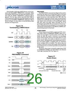
Data for any WRITE burst may be truncated with a
subsequent READ command, and data for a fixed-length
WRITE burst may be immediately followed by a READ
command. Once the READ command is registered, the
data inputs will be ignored, and WRITEs will not be
executed. An example is shown in Figure 17. Data n + 1 is
either the last of a burst of two or the last desired of a
longer burst.
least one clock plus time, regardless of frequency.
In addition, when truncating a WRITE burst, the DQM
signal must be used to mask input data for the clock edge
prior to, and the clock edge coincident with, the
PRECHARGE command. An example is shown in Figure
18. Data n + 1 is either the last of a burst of two or the last
desired of a longer burst. Following the PRECHARGE
command, a subsequent command to the same bank
t
Data for a fixed-length WRITE burst may be followed
by, or truncated with, a PRECHARGE command to the
same bank (provided that auto precharge was not acti-
vated), and a full-page WRITE burst may be truncated
with a PRECHARGE command to the same bank. The
cannot be issued until RP is met.
In the case of a fixed-length burst being executed to
completion, a PRECHARGE command issued at the opti-
mum time (as described above) provides the same op-
eration that would result from the same fixed-length
burst with auto precharge. The disadvantage of the
PRECHARGE command is that it requires that the com-
mand and address buses be available at the appropriate
time to issue the command; the advantage of the
PRECHARGE command is that it can be used to truncate
fixed-length or full-page bursts.
t
PRECHARGE command should be issued WR after the
clock edge at which the last desired input data element is
t
registered. The auto precharge mode requires a WR of at
Figure 16
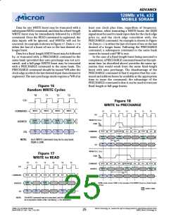
Random WRITE Cycles
T0
T1
T2
T3
CLK
COMMAND
ADDRESS
Figure 18
WRITE to PRECHARGE
WRITE
WRITE
WRITE
WRITE
T0
T1
T2
T3
T4
T5
T6
CLK
t
t
WR@ CK 15ns
BANK,
COL n
BANK,
COL a
BANK,
COL x
BANK,
COL m
DQM
t
RP
D
IN
D
IN
D
IN
DIN
x
NOP
NOP
NOP
WRITE
NOP
PRECHARGE
ACTIVE
COMMAND
ADDRESS
DQ
m
n
a
BANK
(a or all)
BANK a,
COL n
BANK a,
ROW
NOTE:
Each WRITE command may be to any bank.
DQM is LOW.
t
WR
D
n
IN
DIN
n + 1
DQ
t
t
WR@ CK < 15ns
Figure 17
DQM
WRITE to READ
t
RP
T0
T1
T2
T3
T4
T5
NOP
NOP
WRITE
NOP
NOP
PRECHARGE
ACTIVE
COMMAND
ADDRESS
CLK
BANK
(a or all)
BANK a,
COL n
BANK a,
ROW
t
WR
WRITE
NOP
READ
NOP
NOP
NOP
COMMAND
ADDRESS
D
n
IN
DIN
n + 1
DQ
BANK,
COL n
BANK,
COL b
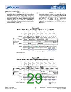
NOTE:
DQM could remain LOW in this example if the WRITE burst is a fixed length
of two.
DON’T CARE
DIN
D
IN
DOUT
DOUT
DQ
n
n + 1
b
b + 1
NOTE:
The WRITE command may be to any bank, and the READ command may
be to any bank. DQM is LOW. CAS latency = 2 for illustration.
128Mb: x16, x32 Mobile SDRAM
MobileY95W_3V_F.p65 – Rev. F; Pub. 9/02
Micron Technology, Inc., reserves the right to change products or specifications without notice.
©2002, Micron Technology, Inc.
25

 MICRON [ MICRON TECHNOLOGY ]