1Gb: x4, x8, x16 DDR2 SDRAM
Electrical Specifications – IDD Parameters
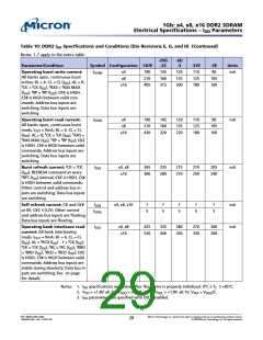
Table 10: DDR2 IDD Specifications and Conditions (Die Revisions E, G, and H) (Continued)
Notes: 1–7 apply to the entire table
-25E/
-25
-3E/
-3
Parameter/Condition
Symbol Configuration -187E
-37E
110
125
180
-5E
90
Units
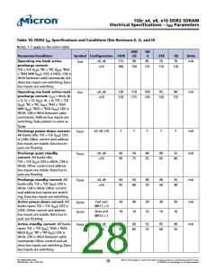
Operating burst write current:
All banks open, continuous burst
writes; BL = 4, CL = CL (IDD), AL = 0;
tCK = tCK (IDD), tRAS = tRAS MAX
(IDD), tRP = tRP (IDD); CKE is HIGH,
CS# is HIGH between valid com-
mands; Address bus inputs are
switching; Data bus inputs are
switching
IDD4W
IDD4R
IDD5
x4
x8
190
210
405
145
160
315
120
135
200
mA
105
160
x16
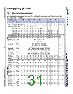
Operating burst read current:
All banks open, continuous burst
reads, IOUT = 0mA; BL = 4, CL = CL
(IDD), AL = 0; tCK = tCK (IDD), tRAS =
tRAS MAX (IDD), tRP = tRP (IDD); CKE
is HIGH, CS# is HIGH between valid
commands; Address bus inputs are
switching; Data bus inputs are
switching
Burst refresh current: tCK = tCK
(IDD); REFRESH command at every
tRFC (IDD) interval; CKE is HIGH, CS#
is HIGH between valid commands;
Other control and address bus in-
puts are switching; Data bus inputs
are switching
x4
x8
190
210
420
145
160
320
120
135
220
110
125
180
90
mA
105
160
x16
x4, x8
x16
265
300
235
280
215
270
210
250
205
240
mA
Self refresh current: CK and CK#
at 0V; CKE ≤ 0.2V; Other control
and address bus inputs are floating;
Data bus inputs are floating
IDD6
x4, x8, x16
7
5
7
5
7
5
7
5
7
5
mA
mA
IDD6L
Operating bank interleave read
current: All bank interleaving
reads, IOUT = 0mA; BL = 4, CL = CL
(IDD), AL = tRCD (IDD) - 1 × tCK (IDD);
tCK = tCK (IDD), tRC = tRC (IDD), tRRD
= tRRD (IDD), tRCD = tRCD (IDD); CKE
is HIGH, CS# is HIGH between valid
commands; Address bus inputs are
stable during deselects; Data bus in-
puts are switching; See on page
for details
IDD7
x4, x8
x16
425
520
335
440
280
350
270
330
260
300
1.
Notes:
IDD specifications are tested after the device is properly initialized. 0°C ≤ TC ≤ +85°C.
2. VDD = +1.8V ±0.1V, VDDQ = +1.8V ±0.1V, VDDL = +1.8V ±0.1V, VREF = VDDQ/2.
3. IDD parameters are specified with ODT disabled.
PDF: 09005aef821ae8bf
1GbDDR2.pdf – Rev. T 02/10 EN
Micron Technology, Inc. reserves the right to change products or specifications without notice.
© 2004 Micron Technology, Inc. All rights reserved.
29

 MICRON [ MICRON TECHNOLOGY ]