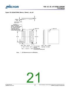
1Gb: x4, x8, x16 DDR2 SDRAM
Ball Assignments and Descriptions
Table 3: FBGA 84-Ball – x16 and 60-Ball – x4, x8 Descriptions
Symbol
Type
Description
A[12:0] (x16)
,A[13:0] (x4, x8)
Input
Address inputs: Provide the row address for ACTIVATE commands, and the column ad-
dress and auto precharge bit (A10) for READ/WRITE commands, to select one location out
of the memory array in the respective bank. A10 sampled during a PRECHARGE com-
mand determines whether the PRECHARGE applies to one bank (A10 LOW, bank selected
by BA[2:0] or all banks (A10 HIGH). The address inputs also provide the op-code during a
LOAD MODE command.
BA[2:0]
CK, CK#
CKE
Input
Input
Input
Bank address inputs: BA[2:0] define to which bank an ACTIVATE, READ, WRITE, or PRE-
CHARGE command is being applied. BA[2:0] define which mode register, including MR,
EMR, EMR(2), and EMR(3), is loaded during the LOAD MODE command.
Clock: CK and CK# are differential clock inputs. All address and control input signals are
sampled on the crossing of the positive edge of CK and negative edge of CK#. Output
data (DQ and DQS/DQS#) is referenced to the crossings of CK and CK#.
Clock enable: CKE (registered HIGH) activates and CKE (registered LOW) deactivates
clocking circuitry on the DDR2 SDRAM. The specific circuitry that is enabled/disabled is
dependent on the DDR2 SDRAM configuration and operating mode. CKE LOW provides
precharge power-down and SELF REFRESH operations (all banks idle), or ACTIVATE power-
down (row active in any bank). CKE is synchronous for power-down entry, power-down
exit, output disable, and for self refresh entry. CKE is asynchronous for self refresh exit.
Input buffers (excluding CK, CK#, CKE, and ODT) are disabled during power-down. Input
buffers (excluding CKE) are disabled during self refresh. CKE is an SSTL_18 input but will
detect a LVCMOS LOW level after VDD is applied during first power-up. After VREF has
become stable during the power-on and initialization sequence, it must be maintained
for proper operation of the CKE receiver. For proper SELF REFRESH operation, VREF must
be maintained.
CS#
Input
Input
Chip select: CS# enables (registered LOW) and disables (registered HIGH) the command
decoder. All commands are masked when CS# is registered high. CS# provides for exter-
nal bank selection on systems with multiple ranks. CS# is considered part of the com-
mand code.
LDM, UDM, DM
Input data mask: DM is an input mask signal for write data. Input data is masked when
DM is sampled HIGH along with that input data during a WRITE access. DM is sampled on
both edges of DQS. Although DM balls are input-only, the DM loading is designed to
match that of DQ and DQS balls. LDM is DM for lower byte DQ[7:0] and UDM is DM for
upper byte DQ[15:8].
ODT
Input
On-die termination: ODT (registered HIGH) enables termination resistance internal to
the DDR2 SDRAM. When enabled, ODT is only applied to each of the following balls:
DQ[15:0], LDM, UDM, LDQS, LDQS#, UDQS, and UDQS# for the x16; DQ[7:0], DQS, DQS#,
RDQS, RDQS#, and DM for the x8; DQ[3:0], DQS, DQS#, and DM for the x4. The ODT input
will be ignored if disabled via the LOAD MODE command.
RAS#, CAS#, WE#
Input
I/O
Command inputs: RAS#, CAS#, and WE# (along with CS#) define the command being
entered.
DQ[15:0] (x16)
DQ[3:0] (x4)
DQ[7:0] (x8)
Data input/output: Bidirectional data bus for 64 Meg x 16.
Bidirectional data bus for 256 Meg x 4.
Bidirectional data bus for 128 Meg x 8.
PDF: 09005aef821ae8bf
1GbDDR2.pdf – Rev. T 02/10 EN
Micron Technology, Inc. reserves the right to change products or specifications without notice.
17
© 2004 Micron Technology, Inc. All rights reserved.

 MICRON [ MICRON TECHNOLOGY ]