2 MEG x 16
ASYNC/PAGE/BURST FLASH MEMORY
READ-WHILE-WRITE/ERASE
CONCURRENCY
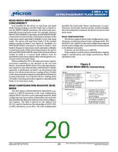
It is possible for the device to read from one bank
while erasing/writing to another bank. Once a bank en-
ters the WRITE/ERASE operation, the other bank auto-
matically enters read array mode. For example, during a
READCONCURRENCYoperation, ifaPROGRAM/ERASE
command is issued in bank a, then bank a changes to the
read status mode and bank b defaults to the read array
mode. The device will read from bank b if the latched
address resides in bank b (see Figure 8). Similarly, if a
PROGRAM/ERASE command is issued in bank b, then
bank b changes to read status mode and bank a defaults
to read array mode. When returning to bank a, the device
will read PROGRAM/ERASE status if the latched address
resides in bank a. A correct bank address must be
specified to read status register after returning from con-
current read in the other bank.
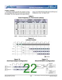
provides the read mode (burst, synchronous, or asyn-
chronous), burstorder, latencycounter, andburstlength.
After executing this command, the device returns to read
array mode.
READ CONFIGURATION
The device supports three read configurations: asyn-
chronous, synchronousburstmode, andpagemode. The
bit RCR15 (see Table 9) in the read configuration register
setsthereadconfiguration. Asynchronousrandommode
is the default read mode.
At power-up, the RCR is set to BBCFh.
Status registers and the device identification register
support asynchronous and single synchronous READ
operations only.
When reading the CFI or the chip protection register,
concurrent operation is not allowed on the top boot
device. Concurrent READ of the CFI or the chip protec-
tion register is only allowed when a PROGRAM or ERASE
operation is performed on bank b on the bottom boot
device. For a bottom boot device, reading of the CFI table
or the chip protection register is only allowed if bank b is
in read array mode. For a top boot device, reading of the
CFI table or the chip protection register is only allowed if
bank a is in read array mode.
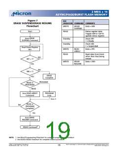
Figure 8
READ-While-WRITE Concurrency
Bank a
Bank b
1 - Erasing/writing to bank a
2 - Erasing in bank a can be
suspended, and a WRITE to
another block in bank a
can be initiated.
1 - Reading from bank b
3 - After the WRITE in that block
is complete, an ERASE can
be resumed by writing an
ERASE RESUME command.
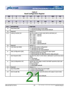
READ CONFIGURATION REGISTER (RCR)
MODE
1 - Reading bank a
1 - Erasing/writing to bank b
2 - Erasing in bank b can be
suspended, and a WRITE to
another block in bank b
can be initiated.
3 - After the WRITE in that block
is complete, an ERASE can
be resumed by writing an
ERASE RESUME command.
The SET READ CONFIGURATION REGISTER com-
mand is a WRITE operation to the read configuration
register(RCR). Itisatwo-cyclecommandsequence. Read
configurationsetupiswritten, followedbyasecondwrite
that specifies the data to be written to the read configura-
tion register. The data is placed on the address bus
A0–A15, and it is latched on the rising edge of ADV#, CE#,
or WE#, whichever occurs first. The read configuration
2 Meg x 16 Async/Page/Burst Flash Memory
MT28F322D20FH_4.p65 – Rev. 4, Pub. 7/02
Micron Technology, Inc., reserves the right to change products or specifications without notice.
©2002, Micron Technology, Inc.
20

 MICRON [ MICRON TECHNOLOGY ]