2 MEG x 16
ASYNC/PAGE/BURST FLASH MEMORY
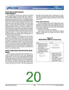
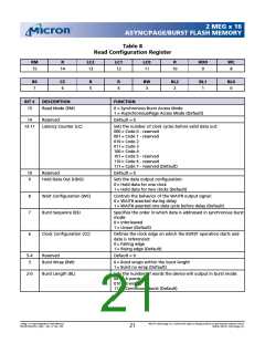
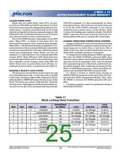
Table 8
Read Configuration Register
RM
R
LC2
LC1
LC0
R
HDO
WC
15
14
13
12
11
10
9
8
BS
CC
R
R
BW
BL2
BL1
BL0
7
6
5
4
3
2
1
0
BIT #
DESCRIPTION
FUNCTION
15
Read Mode (RM)
0 = Synchronous Burst Access Mode
1 = Asynchronous/Page Access Mode (Default)
14
Reserved
Default = 0
13-11
Latency Counter (LC)
Sets the number of clock cycles before valid data out:
000 = Code 0 - reserved
001 = Code 1 - reserved
010 = Code 2
011 = Code 3
100 = Code 4
101 = Code 5 - reserved
110 = Code 6 - reserved
111 = Code 7 - reserved (Default)
10
9
Reserved
Default = 0
Hold Data Out (HDO)
Sets the data output configuration:
0 = Hold data for one clock
1 = Hold data for two clocks (Default)
8
7
Wait Configuration (WC)
Burst Sequence (BS)
Controls the behavior of the WAIT# output signal:
0 = WAIT# asserted during delay
1 = WAIT# asserted one data cycle before delay (Default)
Specifies the order in which data is addressed in synchronous burst
mode:
0 = Interleaved
1 = Linear (Default)
6
Clock Configuration (CC)
Defines the clock edge on which the BURST operation starts and
data is referenced:
0 = Falling edge
1 = Rising edge (Default)
5-4
3
Reserved
Default = 0
Burst Wrap (BW)
0 = Burst wraps within the burst length
1 = Burst no wrap (Default)
2-0
Burst Length (BL)
Sets the number of words the device will output in burst mode:
001 = 4 words
010 = 8 words
111 = Continuous burst (Default)
2 Meg x 16 Async/Page/Burst Flash Memory
MT28F322D20FH_4.p65 – Rev. 4, Pub. 7/02
Micron Technology, Inc., reserves the right to change products or specifications without notice.
21
©2002, Micron Technology, Inc.

 MICRON [ MICRON TECHNOLOGY ]