2 MEG x 16
ASYNC/PAGE/BURST FLASH MEMORY
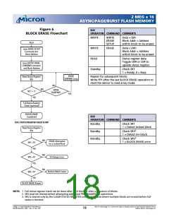
Figure 6
BLOCK ERASE Flowchart
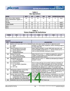
BUS
OPERATION COMMAND COMMENTS
WRITE
WRITE
READ
WRITE
ERASE
SETUP
Data = 20h
Block Addr = Address
within block to be erased
Start
ERASE
Data = D0h
Block Addr = Address
within block to be erased
Issue ERASE SETUP
Command and
Block Address
Status register data
Toggle OE# or CE# to
update status register.
Issue BLOCK ERASE
CONFIRM Command
and Block Address
Standby
Check SR7
1 = Ready, 0 = Busy
ERASE
SUSPEND Loop
Read Status Register
Repeat for subsequent blocks.
Write FFh after the last BLOCK ERASE operation to
reset the device to read array mode.
Bits
NO
ERASE
NO
SR 7 = 1?
SUSPEND?
YES
YES
Full Status Register
1
Check (optional)
BLOCK ERASE
Completed
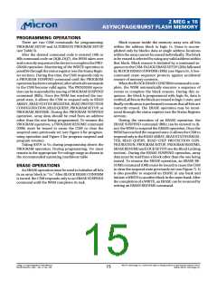
BUS
OPERATION COMMAND COMMENTS
FULL STATUS REGISTER CHECK FLOW
Standby
Standby
Standby
Check SR1
1 = Detect locked block
Check SR32
1 = Detect VPP block
Read Status Register
Bits
Check SR53
NO
ERASE Attempted
on a Locked Block
1 = BLOCK ERASE error
SR1 = 0?
YES
NO
VPP Range Error
SR3 = 0?
YES
NO
BLOCK ERASE Failed
SR5 = 0?
YES
BLOCK ERASE Passed
NOTE: 1. Full status register check can be done after each block or after a sequence of blocks.
2. SR3 must be cleared before attempting additional PROGRAM/ERASE operations.
3. SR5 is cleared only by the CLEAR STATUS REGISTER command in cases where multiple blocks are erased before full
status is checked.
2 Meg x 16 Async/Page/Burst Flash Memory
MT28F322D20FH_4.p65 – Rev. 4, Pub. 7/02
Micron Technology, Inc., reserves the right to change products or specifications without notice.
©2002, Micron Technology, Inc.
18

 MICRON [ MICRON TECHNOLOGY ]