1 Mbit / 2 Mbit / 4 Mbit Multi-Purpose Flash
SST39SF010A / SST39SF020A / SST39SF040
Data Sheet
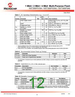
Table 7: DC Operating Characteristics VDD = 4.5-5.5V1
Limits
Max Units Test Conditions
Address input=VILT/VIHT, at f=1/TRC Min
Symbol Parameter
Min
IDD
Power Supply Current
VDD=VDD Max
Read2
25
35
3
mA
mA
mA
CE#=VIL, OE#=WE#=VIH, all I/Os open
CE#=WE#=VIL, OE#=VIH
CE#=VIH, VDD=VDD Max
Program and Erase
ISB1
ISB2
Standby VDD Current
(TTL input)
Standby VDD Current
(CMOS input)
100
µA
CE#=VIHC, VDD=VDD Max
ILI
Input Leakage Current
Output Leakage Current
Input Low Voltage
1
µA
µA
V
VIN=GND to VDD, VDD=VDD Max
VOUT=GND to VDD, VDD=VDD Max
VDD=VDD Min
ILO
10
0.8
VIL
VIH
VIHC
VOL
VOH
Input High Voltage
2.0
V
VDD=VDD Max
Input High Voltage (CMOS)
Output Low Voltage
Output High Voltage
VDD-0.3
V
VDD=VDD Max
0.4
V
IOL=2.1 mA, VDD=VDD Min
IOH=-400 µA, VDD=VDD Min
2.4
V
T7.10 25022
1. Typical conditions for the Active Current shown on the front data sheet page are average values at 25°C
(room temperature), and VDD = 5V for SF devices. Not 100% tested.
2. Values are for 70 ns conditions. See the Multi-Purpose Flash Power Rating application note for further information.
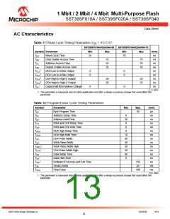
Table 8: Recommended System Power-up Timings
Symbol
Parameter
Minimum
100
Units
µs
1
TPU-READ
Power-up to Read Operation
Power-up to Program/Erase Operation
1
TPU-WRITE
100
µs
T8.1 25022
1. This parameter is measured only for initial qualification and after a design or process change that could affect this
parameter.
Table 9: Capacitance (Ta = 25°C, f=1 Mhz, other pins open)
Parameter
Description
Test Condition
VI/O = 0V
Maximum
12 pF
1
CI/O
I/O Pin Capacitance
Input Capacitance
1
CIN
VIN = 0V
6 pF
T9.0 25022
1. This parameter is measured only for initial qualification and after a design or process change that could affect this
parameter.
Table 10: Reliability Characteristics
Symbol
Parameter
Endurance
Data Retention
Latch Up
Minimum Specification
Units
Cycles
Years
mA
Test Method
1,2
NEND
10,000
100
JEDEC Standard A117
JEDEC Standard A103
JEDEC Standard 78
1
TDR
1
ILTH
100 + IDD
T10.2 25022
1. This parameter is measured only for initial qualification and after a design or process change that could affect this parameter.
2. NEND endurance rating is qualified as a 10,000 cycle minimum for the whole device. A sector- or block-level rating would
result in a higher minimum specification.
©2013 Silicon Storage Technology, Inc.
DS25022B
04/13
12

 MICROCHIP [ MICROCHIP ]