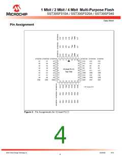
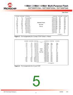
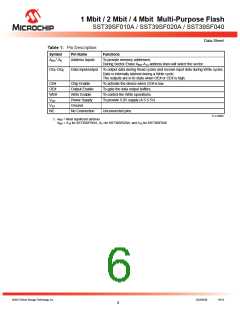
1 Mbit / 2 Mbit / 4 Mbit Multi-Purpose Flash
SST39SF010A / SST39SF020A / SST39SF040
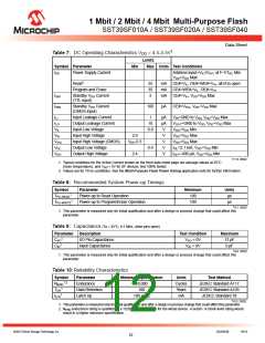
Data Sheet
Write Operation Status Detection
The SST39SF010A/020A/040 provide two software means to detect the completion of a Write (Pro-
gram or Erase) cycle, in order to optimize the system Write cycle time. The software detection includes
two status bits: Data# Polling (DQ7) and Toggle Bit (DQ6). The End-of-Write detection mode is enabled
after the rising edge of WE# which initiates the internal Program or Erase operation.
The actual completion of the nonvolatile write is asynchronous with the system; therefore, either a
Data# Polling or Toggle Bit read may be simultaneous with the completion of the Write cycle. If this
occurs, the system may possibly get an erroneous result, i.e., valid data may appear to conflict with
either DQ7 or DQ6. In order to prevent spurious rejection, if an erroneous result occurs, the software
routine should include a loop to read the accessed location an additional two (2) times. If both reads
are valid, then the device has completed the Write cycle, otherwise the rejection is valid.
Data# Polling (DQ7)
When the SST39SF010A/020A/040 are in the internal Program operation, any attempt to read DQ7 will
produce the complement of the true data. Once the Program operation is completed, DQ7 will produce
true data. Note that even though DQ7 may have valid data immediately following the completion of an
internal Write operation, the remaining data outputs may still be invalid: valid data on the entire data
bus will appear in subsequent successive Read cycles after an interval of 1 µs. During internal Erase
operation, any attempt to read DQ7 will produce a ‘0’. Once the internal Erase operation is completed,
DQ7 will produce a ‘1’. The Data# Polling is valid after the rising edge of fourth WE# (or CE#) pulse for
Program operation. For Sector- or Chip-Erase, the Data# Polling is valid after the rising edge of sixth
WE# (or CE#) pulse. See Figure 8 for Data# Polling timing diagram and Figure 17 for a flowchart.
Toggle Bit (DQ6)
During the internal Program or Erase operation, any consecutive attempts to read DQ6 will produce
alternating 0s and 1s, i.e., toggling between 0 and 1. When the internal Program or Erase operation is
completed, the toggling will stop. The device is then ready for the next operation. The Toggle Bit is valid
after the rising edge of fourth WE# (or CE#) pulse for Program operation. For Sector- or Chip-Erase,
the Toggle Bit is valid after the rising edge of sixth WE# (or CE#) pulse. See Figure 9 for Toggle Bit tim-
ing diagram and Figure 17 for a flowchart.
Data Protection
The SST39SF010A/020A/040 provide both hardware and software features to protect nonvolatile data
from inadvertent writes.
Hardware Data Protection
Noise/Glitch Protection: A WE# or CE# pulse of less than 5 ns will not initiate a Write cycle.
V
DD Power Up/Down Detection: The Write operation is inhibited when VDD is less than 2.5V.
Write Inhibit Mode: Forcing OE# low, CE# high, or WE# high will inhibit the Write operation. This pre-
vents inadvertent writes during power-up or power-down.
©2013 Silicon Storage Technology, Inc.
DS25022B
04/13
8

 MICROCHIP [ MICROCHIP ]