1 Mbit / 2 Mbit / 4 Mbit Multi-Purpose Flash
SST39SF010A / SST39SF020A / SST39SF040
Data Sheet
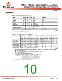
Operations
Table 3: Operation Modes Selection
Mode
CE#
VIL
VIL
VIL
VIH
X
OE#
VIL
VIH
VIH
X
WE#
VIH
VIL
VIL
X
DQ
Address
Read
DOUT
AIN
Program
Erase
DIN
X1
AIN
Sector address, XXH for Chip-Erase
Standby
Write Inhibit
High Z
High Z/ DOUT
High Z/ DOUT
X
X
X
VIL
X
X
X
VIH
Product Identification
Software Mode
VIL
VIL
VIH
See Table 4
T3.3 25022
1. X can be VIL or VIH, but no other value.
Table 4: Software Command Sequence
Command
Sequence
1st Bus
Write Cycle
2nd Bus
Write Cycle
3rd Bus
Write Cycle
4th Bus
Write Cycle
5th Bus
Write Cycle
6th Bus
Write Cycle
Addr1 Data Addr1 Data Addr1 Data Addr1 Data Addr1 Data Addr1 Data
5555H AAH 2AAAH 55H 5555H A0H Data
BA2
5555H AAH 2AAAH 55H 5555H 80H 5555H AAH 2AAAH 55H SAX
5555H AAH 2AAAH 55H 5555H 80H 5555H AAH 2AAAH 55H 5555H 10H
Byte-Program
Sector-Erase
Chip-Erase
3
30H
Software ID Entry4,5 5555H AAH 2AAAH 55H 5555H 90H
Software ID Exit6
Software ID Exit6
XXH F0H
5555H AAH 2AAAH 55H 5555H F0H
T4.2 25022
1. Address format A14-A0 (Hex), Addresses AMS-A15 can be VIL or VIH, but no other value, for the Command sequence.
AMS = Most significant address
A
MS = A16 for SST39SF010A, A17 for SST39SF020A, and A18 for SST39SF040
2. BA = Program Byte address
3. SAX for Sector-Erase; uses AMS-A12 address lines
4. The device does not remain in Software Product ID mode if powered down.
5. With AMS-A1 = 0; SST Manufacturer’s ID = BFH, is read with A0 = 0,
SST39SF010A Device ID = B5H, is read with A0 = 1
SST39SF020A Device ID = B6H, is read with A0 = 1
SST39SF040 Device ID = B7H, is read with A0 = 1
6. Both Software ID Exit operations are equivalent
©2013 Silicon Storage Technology, Inc.
DS25022B
04/13
10

 MICROCHIP [ MICROCHIP ]