PIC24FJ64GA104 FAMILY
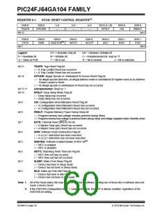
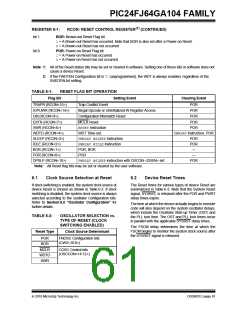
REGISTER 6-1:
RCON: RESET CONTROL REGISTER(1) (CONTINUED)
bit 1
BOR: Brown-out Reset Flag bit
1= A Brown-out Reset has occurred. Note that BOR is also set after a Power-on Reset.
0= A Brown-out Reset has not occurred
bit 0
POR: Power-on Reset Flag bit
1= A Power-on Reset has occurred
0= A Power-on Reset has not occurred
Note 1: All of the Reset status bits may be set or cleared in software. Setting one of these bits in software does not
cause a device Reset.
2: If the FWDTEN Configuration bit is ‘1’ (unprogrammed), the WDT is always enabled, regardless of the
SWDTEN bit setting.
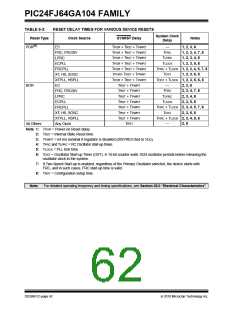
TABLE 6-1:
RESET FLAG BIT OPERATION
Setting Event
Flag Bit
Clearing Event
TRAPR (RCON<15>)
IOPUWR (RCON<14>)
CM (RCON<9>)
Trap Conflict Event
POR
Illegal Opcode or Uninitialized W Register Access
Configuration Mismatch Reset
MCLR Reset
POR
POR
EXTR (RCON<7>)
SWR (RCON<6>)
WDTO (RCON<4>)
SLEEP (RCON<3>)
IDLE (RCON<2>)
BOR (RCON<1>)
POR (RCON<0>)
DPSLP (RCON<10>)
POR
RESETInstruction
POR
WDT Time-out
PWRSAVInstruction, POR
PWRSAV #SLEEPInstruction
PWRSAV #IDLEInstruction
POR, BOR
POR
POR
—
POR
—
PWRSAV #SLEEPinstruction with DSCON <DSEN> set
POR
Note: All Reset flag bits may be set or cleared by the user software.
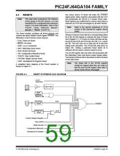
6.1
Clock Source Selection at Reset
6.2
Device Reset Times
If clock switching is enabled, the system clock source at
device Reset is chosen as shown in Table 6-2. If clock
switching is disabled, the system clock source is always
selected according to the oscillator Configuration bits.
Refer to Section 8.0 “Oscillator Configuration” for
further details.
The Reset times for various types of device Reset are
summarized in Table 6-3. Note that the System Reset
signal, SYSRST, is released after the POR and PWRT
delay times expire.
The time at which the device actually begins to execute
code will also depend on the system oscillator delays,
which include the Oscillator Start-up Timer (OST) and
the PLL lock time. The OST and PLL lock times occur
in parallel with the applicable SYSRST delay times.
TABLE 6-2:
OSCILLATOR SELECTION vs.
TYPE OF RESET (CLOCK
SWITCHING ENABLED)
The FSCM delay determines the time at which the
FSCM begins to monitor the system clock source after
the SYSRST signal is released.
Reset Type
Clock Source Determinant
POR
BOR
FNOSC Configuration bits
(CW2<10:8>)
MCLR
WDTO
SWR
COSC Control bits
(OSCCON<14:12>)
2010 Microchip Technology Inc.
DS39951C-page 61

 MICROCHIP [ MICROCHIP ]