PIC24FJ64GA104 FAMILY
instructions write the desired data into the write latches
and specify the lower 16 bits of the program memory
address to write to. To configure the NVMCON register
for a word write, set the NVMOP bits (NVMCON<3:0>)
to ‘0011’. The write is performed by executing the
unlock sequence and setting the WR bit (see
Example 5-7).
5.6.2
PROGRAMMING A SINGLE WORD
OF FLASH PROGRAM MEMORY
If a Flash location has been erased, it can be pro-
grammed using table write instructions to write an
instruction word (24-bit) into the write latch. The
TBLPAG register is loaded with the 8 Most Significant
Bytes of the Flash address. The TBLWTLand TBLWTH
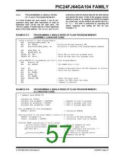
EXAMPLE 5-7:
PROGRAMMING A SINGLE WORD OF FLASH PROGRAM MEMORY
(ASSEMBLY LANGUAGE CODE)
; Setup a pointer to data Program Memory
MOV
MOV
MOV
#tblpage(PROG_ADDR), W0
W0, TBLPAG
#tbloffset(PROG_ADDR), W0
;
;Initialize PM Page Boundary SFR
;Initialize a register with program memory address
MOV
MOV
#LOW_WORD, W2
#HIGH_BYTE, W3
;
;
TBLWTL W2, [W0]
TBLWTH W3, [W0++]
; Write PM low word into program latch
; Write PM high byte into program latch
; Setup NVMCON for programming one word to data Program Memory
MOV
MOV
#0x4003, W0
W0, NVMCON
;
; Set NVMOP bits to 0011
DISI
MOV
MOV
MOV
MOV
BSET
NOP
NOP
#5
; Disable interrupts while the KEY sequence is written
; Write the key sequence
#0x55, W0
W0, NVMKEY
#0xAA, W0
W0, NVMKEY
NVMCON, #WR
; Start the write cycle
; Insert two NOPs after the erase
; Command is asserted
EXAMPLE 5-8:
PROGRAMMING A SINGLE WORD OF FLASH PROGRAM MEMORY
(C LANGUAGE CODE)
// C example using MPLAB C30
unsigned int offset;
unsigned long progAddr = 0xXXXXXX;
unsigned int progDataL = 0xXXXX;
unsigned char progDataH = 0xXX;
// Address of word to program
// Data to program lower word
// Data to program upper byte
//Set up NVMCON for word programming
NVMCON = 0x4003;
// Initialize NVMCON
//Set up pointer to the first memory location to be written
TBLPAG = progAddr>>16;
// Initialize PM Page Boundary SFR
offset = progAddr & 0xFFFF;
// Initialize lower word of address
//Perform TBLWT instructions to write latches
__builtin_tblwtl(offset, progDataL);
__builtin_tblwth(offset, progDataH);
asm(“DISI #5”);
// Write to address low word
// Write to upper byte
// Block interrupts with priority < 7
// for next 5 instructions
// C30 function to perform unlock
// sequence and set WR
__builtin_write_NVM();
2010 Microchip Technology Inc.
DS39951C-page 57

 MICROCHIP [ MICROCHIP ]