PIC24FJ64GA104 FAMILY
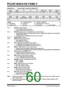
REGISTER 6-1:
RCON: RESET CONTROL REGISTER(1)
R/W-0
R/W-0
U-0
—
U-0
—
U-0
—
R/CO-0, HS
DPSLP
R/W-0
CM
R/W-0
TRAPR
bit 15
IOPUWR
PMSLP
bit 8
R/W-0
EXTR
R/W-0
SWR
R/W-0
SWDTEN(2)
R/W-0
WDTO
R/W-0,
SLEEP
R/W-0
IDLE
R/W-1
BOR
R/W-1
POR
bit 7
bit 0
Legend:
CO = Clearable Only bit
W = Writable bit
HS = Hardware Settable bit
U = Unimplemented bit, read as ‘0’
‘0’ = Bit is cleared x = Bit is unknown
R = Readable bit
-n = Value at POR
‘1’ = Bit is set
bit 15
bit 14
TRAPR: Trap Reset Flag bit
1= A Trap Conflict Reset has occurred
0= A Trap Conflict Reset has not occurred
IOPUWR: Illegal Opcode or Uninitialized W Access Reset Flag bit
1= An illegal opcode detection, an illegal address mode or uninitialized W register used as an Address
Pointer caused a Reset
0= An illegal opcode or uninitialized W Reset has not occurred
bit 13-11
bit 10
Unimplemented: Read as ‘0’
DPSLP: Deep Sleep Mode Flag bit
1= Deep Sleep has occurred
0= Deep Sleep has not occurred
bit 9
bit 8
bit 7
bit 6
bit 5
bit 4
bit 3
bit 2
CM: Configuration Word Mismatch Reset Flag bit
1= A Configuration Word Mismatch Reset has occurred
0= A Configuration Word Mismatch Reset has not occurred
PMSLP: Program Memory Power During Sleep bit
1= Program memory bias voltage remains powered during Sleep
0= Program memory bias voltage is powered down during Sleep and voltage regulator enters Standby mode
EXTR: External Reset (MCLR) Pin bit
1= A Master Clear (pin) Reset has occurred
0= A Master Clear (pin) Reset has not occurred
SWR: Software Reset (Instruction) Flag bit
1= A RESETinstruction has been executed
0= A RESETinstruction has not been executed
SWDTEN: Software Enable/Disable of WDT bit(2)
1= WDT is enabled
0= WDT is disabled
WDTO: Watchdog Timer Time-out Flag bit
1= WDT time-out has occurred
0= WDT time-out has not occurred
SLEEP: Wake From Sleep Flag bit
1= Device has been in Sleep mode
0= Device has not been in Sleep mode
IDLE: Wake-up From Idle Flag bit
1= Device has been in Idle mode
0= Device has not been in Idle mode
Note 1: All of the Reset status bits may be set or cleared in software. Setting one of these bits in software does not
cause a device Reset.
2: If the FWDTEN Configuration bit is ‘1’ (unprogrammed), the WDT is always enabled, regardless of the
SWDTEN bit setting.
DS39951C-page 60
2010 Microchip Technology Inc.

 MICROCHIP [ MICROCHIP ]