PIC24FJ64GA104 FAMILY
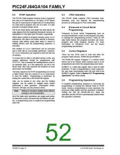
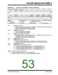
REGISTER 5-1:
NVMCON: FLASH MEMORY CONTROL REGISTER
R/SO-0, HC(1) R/W-0(1) R/W-0, HS(1)
U-0
—
U-0
—
U-0
—
U-0
—
U-0
—
WR
bit 15
WREN
WRERR
bit 8
U-0
—
R/W-0(1)
ERASE
U-0
—
U-0
—
R/W-0(1)
NVMOP3(2)
R/W-0(1)
NVMOP2(2)
R/W-0(1)
NVMOP1(2) NVMOP0(2)
R/W-0(1)
bit 7
bit 0
Legend:
SO = Settable Only bit
W = Writable bit
‘1’ = Bit is set
HC = Hardware Clearable bit
HS = Hardware Settable bit
R = Readable bit
U = Unimplemented bit, read as ‘0’
‘0’ = Bit is cleared x = Bit is unknown
-n = Value at POR
bit 15
WR: Write Control bit(1)
1= Initiates a Flash memory program or erase operation. The operation is self-timed and the bit is
cleared by hardware once the operation is complete.
0= Program or erase operation is complete and inactive
bit 14
bit 13
WREN: Write Enable bit(1)
1= Enable Flash program/erase operations
0= Inhibit Flash program/erase operations
WRERR: Write Sequence Error Flag bit(1)
1= An improper program or erase sequence attempt, or termination has occurred (bit is set
automatically on any set attempt of the WR bit)
0= The program or erase operation completed normally
bit 12-7
bit 6
Unimplemented: Read as ‘0’
ERASE: Erase/Program Enable bit(1)
1= Perform the erase operation specified by NVMOP<3:0> on the next WR command
0= Perform the program operation specified by NVMOP<3:0> on the next WR command
bit 5-4
bit 3-0
Unimplemented: Read as ‘0’
NVMOP<3:0>: NVM Operation Select bits(1,2)
1111= Memory bulk erase operation (ERASE = 1) or no operation (ERASE = 0)(3)
0011= Memory word program operation (ERASE = 0) or no operation (ERASE = 1)
0010= Memory page erase operation (ERASE = 1) or no operation (ERASE = 0)
0001= Memory row program operation (ERASE = 0) or no operation (ERASE = 1)
Note 1: These bits can only be reset on POR.
2: All other combinations of NVMOP<3:0> are unimplemented.
3: Available in ICSP™ mode only. Refer to device programming specification.
2010 Microchip Technology Inc.
DS39951C-page 53

 MICROCHIP [ MICROCHIP ]