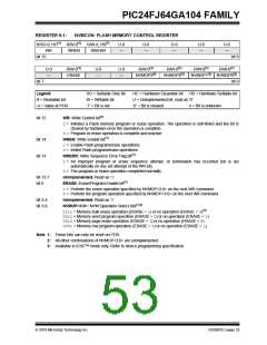
PIC24FJ64GA104 FAMILY
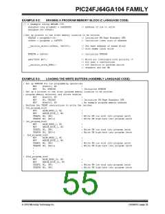
RTSP is accomplished using TBLRD (table read) and
TBLWT (table write) instructions. With RTSP, the user
5.0
FLASH PROGRAM MEMORY
Note:
This data sheet summarizes the features
of this group of PIC24F devices. It is not
intended to be a comprehensive reference
source. For more information, refer to the
“PIC24F Family Reference Manual”,
may write program memory data in blocks of 64 instruc-
tions (192 bytes) at a time and erase program memory
in blocks of 512 instructions (1536 bytes) at a time.
5.1
Table Instructions and Flash
Programming
Section
4.
“Program
Memory”
(DS39715).
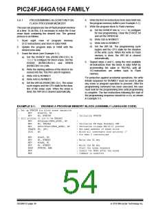
Regardless of the method used, all programming of
Flash memory is done with the table read and table
write instructions. These allow direct read and write
access to the program memory space from the data
memory while the device is in normal operating mode.
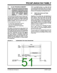
The 24-bit target address in the program memory is
formed using the TBLPAG<7:0> bits and the Effective
Address (EA) from a W register specified in the table
instruction, as shown in Figure 5-1.
The PIC24FJ64GA104 family of devices contains inter-
nal Flash program memory for storing and executing
application code. The memory is readable, writable and
erasable when operating with VDD over 2.35V. (If the
regulator is disabled, VDDCORE must be over 2.25V.)
It can be programmed in four ways:
• In-Circuit Serial Programming™ (ICSP™)
• Run-Time Self-Programming (RTSP)
The TBLRDLand the TBLWTLinstructions are used to
read or write to bits<15:0> of program memory.
TBLRDLand TBLWTLcan access program memory in
both Word and Byte modes.
• Enhanced In-Circuit Serial Programming
(Enhanced ICSP)
ICSP allows a PIC24FJ64GA104 family device to be
serially programmed while in the end application circuit.
This is simply done with two lines for the programming
clock and programming data (which are named PGECx
and PGEDx, respectively), and three other lines for
power (VDD), ground (VSS) and Master Clear (MCLR).
This allows customers to manufacture boards with
unprogrammed devices and then program the micro-
controller just before shipping the product. This also
allows the most recent firmware or a custom firmware
to be programmed.
The TBLRDHand TBLWTHinstructions are used to read
or write to bits<23:16> of program memory. TBLRDH
and TBLWTHcan also access program memory in Word
or Byte mode.
FIGURE 5-1:
ADDRESSING FOR TABLE REGISTERS
24 Bits
Program Counter
Using
Program
Counter
0
0
Working Reg EA
Using
Table
Instruction
1/0
TBLPAG Reg
8 Bits
16 Bits
User/Configuration
Space Select
Byte
Select
24-Bit EA
2010 Microchip Technology Inc.
DS39951C-page 51

 MICROCHIP [ MICROCHIP ]