PIC24FJ64GA104 FAMILY
4. Write the first 64 instructions from data RAM into
the program memory buffers (see Example 5-1).
5.6.1
PROGRAMMING ALGORITHM FOR
FLASH PROGRAM MEMORY
5. Write the program block to Flash memory:
The user can program one row of Flash program memory
at a time. To do this, it is necessary to erase the 8-row
erase block containing the desired row. The general
process is as follows:
a) Set the NVMOP bits to ‘0001’ to configure
for row programming. Clear the ERASE bit
and set the WREN bit.
b) Write 55h to NVMKEY.
c) Write AAh to NVMKEY.
1. Read eight rows of program memory
(512 instructions) and store in data RAM.
d) Set the WR bit. The programming cycle
begins and the CPU stalls for the duration
of the write cycle. When the write to Flash
memory is done, the WR bit is cleared
automatically.
2. Update the program data in RAM with the
desired new data.
3. Erase the block (see Example 5-1):
a) Set the NVMOP bits (NVMCON<3:0>) to
‘0010’ to configure for block erase. Set the
ERASE (NVMCON<6>) and WREN
(NVMCON<14>) bits.
6. Repeat steps 4 and 5, using the next available
64 instructions from the block in data RAM by
incrementing the value in TBLPAG, until all
512 instructions are written back to Flash
memory.
b) Write the starting address of the block to be
erased into the TBLPAG and W registers.
c) Write 55h to NVMKEY.
d) Write AAh to NVMKEY.
For protection against accidental operations, the write
initiate sequence for NVMKEY must be used to allow
any erase or program operation to proceed. After the
programming command has been executed, the user
must wait for the programming time until programming
is complete. The two instructions following the start of
the programming sequence should be NOPs, as shown
in Example 5-5.
e) Set the WR bit (NVMCON<15>). The erase
cycle begins and the CPU stalls for the dura-
tion of the erase cycle. When the erase is
done, the WR bit is cleared automatically.
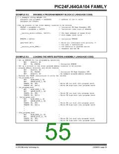
EXAMPLE 5-1:
ERASING A PROGRAM MEMORY BLOCK (ASSEMBLY LANGUAGE CODE)
; Set up NVMCON for block erase operation
MOV
MOV
#0x4042, W0
W0, NVMCON
;
; Initialize NVMCON
; Init pointer to row to be ERASED
MOV
MOV
MOV
#tblpage(PROG_ADDR), W0
W0, TBLPAG
#tbloffset(PROG_ADDR), W0
;
; Initialize PM Page Boundary SFR
; Initialize in-page EA[15:0] pointer
; Set base address of erase block
; Block all interrupts with priority <7
; for next 5 instructions
TBLWTL W0, [W0]
DISI
#5
MOV
MOV
MOV
MOV
BSET
NOP
NOP
#0x55, W0
W0, NVMKEY
#0xAA, W1
W1, NVMKEY
NVMCON, #WR
; Write the 55 key
;
; Write the AA key
; Start the erase sequence
; Insert two NOPs after the erase
; command is asserted
DS39951C-page 54
2010 Microchip Technology Inc.

 MICROCHIP [ MICROCHIP ]