PIC24FJ64GA104 FAMILY
5.2
RTSP Operation
5.3
JTAG Operation
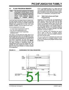
The PIC24F Flash program memory array is organized
into rows of 64 instructions or 192 bytes. RTSP allows
the user to erase blocks of eight rows (512 instructions)
at a time and to program one row at a time. It is also
possible to program single words.
The PIC24F family supports JTAG boundary scan.
Boundary scan can improve the manufacturing
process by verifying pin to PCB connectivity.
5.4
Enhanced In-Circuit Serial
Programming
The 8-row erase blocks and single row write blocks are
edge-aligned, from the beginning of program memory, on
boundaries of 1536 bytes and 192 bytes, respectively.
Enhanced In-Circuit Serial Programming uses an
on-board bootloader, known as the program executive,
to manage the programming process. Using an SPI
data frame format, the program executive can erase,
program and verify program memory. For more
information on Enhanced ICSP, see the device
programming specification.
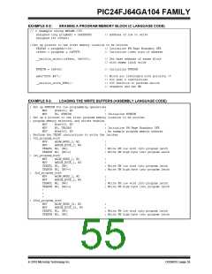
When data is written to program memory using TBLWT
instructions, the data is not written directly to memory.
Instead, data written using table writes is stored in
holding latches until the programming sequence is
executed.
Any number of TBLWT instructions can be executed
and a write will be successfully performed. However,
64 TBLWTinstructions are required to write the full row
of memory.
5.5
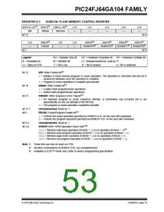
Control Registers
There are two SFRs used to read and write the
program Flash memory: NVMCON and NVMKEY.
To ensure that no data is corrupted during a write, any
unused addresses should be programmed with
FFFFFFh. This is because the holding latches reset to
an unknown state, so if the addresses are left in the
Reset state, they may overwrite the locations on rows
which were not rewritten.
The NVMCON register (Register 5-1) controls which
blocks are to be erased, which memory type is to be
programmed and when the programming cycle starts.
NVMKEY is a write-only register that is used for write
protection. To start a programming or erase sequence,
the user must consecutively write 55h and AAh to the
NVMKEY register. Refer to Section 5.6 “Programming
Operations” for further details.
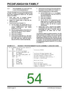
The basic sequence for RTSP programming is to set up
a Table Pointer, then do a series of TBLWTinstructions
to load the buffers. Programming is performed by
setting the control bits in the NVMCON register.
5.6
Programming Operations
Data can be loaded in any order and the holding
registers can be written to multiple times before
performing a write operation. Subsequent writes,
however, will wipe out any previous writes.
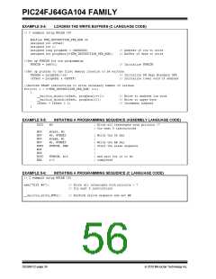
A complete programming sequence is necessary for
programming or erasing the internal Flash in RTSP
mode. During a programming or erase operation, the
processor stalls (waits) until the operation is finished.
Setting the WR bit (NVMCON<15>) starts the
operation and the WR bit is automatically cleared when
the operation is finished.
Note:
Writing to a location multiple times without
erasing is not recommended.
All of the table write operations are single-word writes
(2 instruction cycles), because only the buffers are writ-
ten. A programming cycle is required for programming
each row.
DS39951C-page 52
2010 Microchip Technology Inc.

 MICROCHIP [ MICROCHIP ]