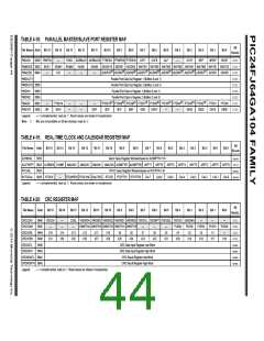
TABLE 4-23: SYSTEM REGISTER MAP
All
Resets
File Name Addr
Bit 15
Bit 14
Bit 13
Bit 12
Bit 11
Bit 10
Bit 9
Bit 8
Bit 7
Bit 6
Bit 5
Bit 4
Bit 3
Bit 2
Bit 1
Bit 0
RCON
0740
0742
0744
0748
TRAPR IOPUWR
—
—
—
—
DPSLP
NOSC2
CM
PMSLP
EXTR
SWR
SWDTEN WDTO
SLEEP
CF
IDLE
BOR
POR
Note 1
OSCCON
CLKDIV
OSCTUN
—
ROI
—
COSC2
DOZE2
—
COSC1
DOZE1
—
COSC0
DOZE0
—
NOSC1
NOSC0 CLKLOCK IOLOCK
LOCK
—
—
—
POSCEN SOSCEN OSWEN Note 2
DOZEN RCDIV2 RCDIV1 RCDIV0
—
—
—
—
—
—
—
—
TUN2
—
—
TUN1
—
—
TUN0
—
0100
0000
0000
—
—
—
—
TUN5
—
TUN4
—
TUN3
—
REFOCON 074E
ROEN
—
ROSSLP ROSEL RODIV3 RODIV2 RODIV1 RODIV0
Legend:
Note 1:
2:
— = unimplemented, read as ‘0’. Reset values are shown in hexadecimal.
The Reset value of the RCON register is dependent on the type of Reset event. See Section 6.0 “Resets” for more information.
The Reset value of the OSCCON register is dependent on both the type of Reset event and the device configuration. See Section 8.0 “Oscillator Configuration” for more information.
TABLE 4-24: DEEP SLEEP REGISTER MAP
All
Resets(1)
File Name Addr
Bit 15
Bit 14
Bit 13
Bit 12
Bit 11
Bit 10
Bit 9
Bit 8
Bit 7
Bit 6
Bit 5
Bit 4
Bit 3
Bit 2
Bit 1
Bit 0
DSCON
758
DSEN
—
—
—
—
—
—
—
—
—
—
—
—
—
—
—
—
—
—
—
—
—
—
DSBOR RELEASE 0000
DSWAKE
DSGPR0
DSGPR1
075A
075C
075E
DSINT0
DSFLT
DSWDT DSRTC DSMCLR
—
DSPOR
0001
0000
0000
Deep Sleep General Purpose Register 0
Deep Sleep General Purpose Register 1
Legend:
Note 1:
— = unimplemented, read as ‘0’. Reset values are shown in hexadecimal.
The Deep Sleep registers are only reset on a VDD POR event.
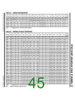
TABLE 4-25: NVM REGISTER MAP
All
Resets
File Name Addr
Bit 15
Bit 14
Bit 13
Bit 12
Bit 11
Bit 10
Bit 9
Bit 8
Bit 7
Bit 6
Bit 5
Bit 4
Bit 3
Bit 2
Bit 1
Bit 0
NVMCON
NVMKEY
0760
0766
WR
—
WREN
—
WRERR
—
—
—
—
—
—
—
—
—
—
—
—
ERASE
—
—
NVMOP3 NVMOP2 NVMOP1 NVMOP0 0000(1)
NVMKEY Register<7:0>
0000
Legend:
Note 1:
— = unimplemented, read as ‘0’. Reset values are shown in hexadecimal.
Reset value shown is for POR only. Value on other Reset states is dependent on the state of memory write or erase operations at the time of Reset.
TABLE 4-26: PMD REGISTER MAP
All
Resets
File Name Addr
Bit 15
Bit 14
Bit 13
Bit 12
Bit 11
Bit 10
Bit 9
Bit 8
Bit 7
Bit 6
Bit 5
Bit 4
Bit 3
Bit 2
Bit 1
Bit 0
PMD1
PMD2
PMD3
PMD4
Legend:
0770
0772
0774
0776
T5MD
—
T4MD
—
T3MD
—
T2MD
IC5MD
—
T1MD
IC4MD
—
—
—
—
I2C1MD
—
U2MD
—
U1MD
—
SPI2MD SPI1MD
—
—
ADC1MD 0000
IC3MD
IC2MD
IC1MD
OC5MD OC4MD OC3MD OC2MD OC1MD
0000
0000
0000
—
—
—
CMPMD RTCCMD PMPMD CRCMD
—
—
—
—
—
—
I2C2MD
—
—
—
—
—
—
—
—
—
—
—
—
—
REFOMD CTMUMD LVDMD
— = unimplemented, read as ‘0’. Reset values are shown in hexadecimal.

 MICROCHIP [ MICROCHIP ]