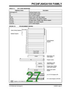
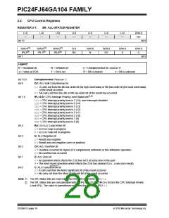
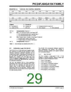
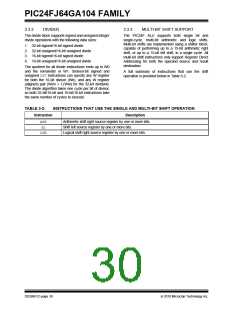
PIC24FJ64GA104 FAMILY
from either the 23-bit Program Counter (PC) during pro-
gram execution, or from table operation or data space
remapping, as described in Section 4.3 “Interfacing
Program and Data Memory Spaces”.
4.0
MEMORY ORGANIZATION
As Harvard architecture devices, PIC24F micro-
controllers feature separate program and data memory
spaces and busses. This architecture also allows the
direct access of program memory from the data space
during code execution.
User access to the program memory space is restricted
to the lower half of the address range (000000h to
7FFFFFh). The exception is the use of TBLRD/TBLWT
operations which use TBLPAG<7> to permit access to
the Configuration bits and Device ID sections of the
configuration memory space.
4.1
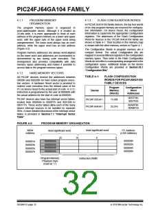
Program Address Space
The program address memory space of the
PIC24FJ64GA104 family devices is 4M instructions.
The space is addressable by a 24-bit value derived
Memory maps for the PIC24FJ64GA104 family of
devices are shown in Figure 4-1.
FIGURE 4-1:
PROGRAM SPACE MEMORY MAP FOR PIC24FJ64GA104 FAMILY DEVICES
PIC24FJ32GA10X
PIC24FJ64GA10X
000000h
000002h
000004h
GOTOInstruction
Reset Address
GOTOInstruction
Reset Address
Interrupt Vector Table
Reserved
Interrupt Vector Table
Reserved
0000FEh
000100h
000104h
0001FEh
000200h
Alternate Vector Table
Alternate Vector Table
User Flash
Program Memory
(11K instructions)
User Flash
Program Memory
(22K instructions)
Flash Config Words
0057FEh
005800h
Flash Config Words
00ABFEh
00AC00h
Unimplemented
Read ‘0’
Unimplemented
Read ‘0’
7FFFFFh
800000h
Reserved
Reserved
F7FFFEh
F80000h
Device Config Registers
Reserved
Device Config Registers
Reserved
F8000Eh
F80010h
FEFFFEh
FF0000h
DEVID (2)
DEVID (2)
FFFFFFh
Note:
Memory areas are not shown to scale.
2010 Microchip Technology Inc.
DS39951C-page 31

 MICROCHIP [ MICROCHIP ]