PIC24FJ64GA104 FAMILY
A Sign-Extend (SE) instruction is provided to allow
users to translate 8-bit signed data to 16-bit signed
values. Alternatively, for 16-bit unsigned data, users
can clear the MSB of any W register by executing a
Zero-Extend (ZE) instruction on the appropriate
address.
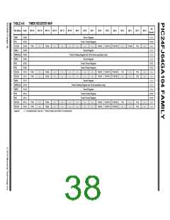
4.2.2
DATA MEMORY ORGANIZATION
AND ALIGNMENT
To maintain backward compatibility with PIC® devices
and improve data space memory usage efficiency, the
PIC24F instruction set supports both word and byte
operations. As a consequence of byte accessibility, all
Effective Address calculations are internally scaled to
step through word-aligned memory. For example, the
core recognizes that Post-Modified Register Indirect
Addressing mode [Ws++] will result in a value of Ws + 1
for byte operations and Ws + 2 for word operations.
Although most instructions are capable of operating on
word or byte data sizes, it should be noted that some
instructions operate only on words.
4.2.3
NEAR DATA SPACE
The 8-Kbyte area between 0000h and 1FFFh is
referred to as the near data space. Locations in this
space are directly addressable via a 13-bit absolute
address field within all memory direct instructions. The
remainder of the data space is indirectly addressable.
Additionally, the whole data space is addressable using
MOV instructions, which support Memory Direct
Addressing with a 16-bit address field.
Data byte reads will read the complete word which con-
tains the byte using the LSb of any EA to determine
which byte to select. The selected byte is placed onto
the LSB of the data path. That is, data memory and reg-
isters are organized as two parallel, byte-wide entities
with shared (word) address decode, but separate write
lines. Data byte writes only write to the corresponding
side of the array or register which matches the byte
address.
4.2.4
SFR SPACE
All word accesses must be aligned to an even address.
Misaligned word data fetches are not supported, so
care must be taken when mixing byte and word
operations or translating from 8-bit MCU code. If a
misaligned read or write is attempted, an address error
trap will be generated. If the error occurred on a read,
the instruction underway is completed; if it occurred on
a write, the instruction will be executed but the write will
not occur. In either case, a trap is then executed, allow-
ing the system and/or user to examine the machine
state prior to execution of the address Fault.
The first 2 Kbytes of the near data space, from 0000h
to 07FFh, are primarily occupied with Special Function
Registers (SFRs). These are used by the PIC24F core
and peripheral modules for controlling the operation of
the device.
SFRs are distributed among the modules that they
control and are generally grouped together by module.
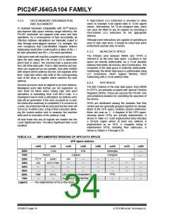
Much of the SFR space contains unused addresses;
these are read as ‘0’. A diagram of the SFR space,
showing where SFRs are actually implemented, is
shown in Table 4-2. Each implemented area indicates
a 32-byte region where at least one address is
implemented as an SFR. A complete listing of
implemented SFRs, including their addresses, is
shown in Tables 4-3 through 4-26.
All byte loads into any W register are loaded into the
Least Significant Byte. The Most Significant Byte is not
modified.
TABLE 4-2:
IMPLEMENTED REGIONS OF SFR DATA SPACE
SFR Space Address
xx00
xx20
xx40
xx60
xx80
xxA0
xxC0
xxE0
000h
100h
200h
300h
400h
500h
600h
700h
Core
ICN
Interrupts
—
—
Timers
Capture
Compare
I2C™
A/D
—
UART
SPI
—
—
—
—
—
—
—
—
—
—
—
I/O
A/D/CTMU
—
—
—
—
—
—
—
—
—
—
—
—
—
—
—
PMP
—
RTCC
—
CRC/Comp Comparators
System/DS NVM/PMD
PPS
—
—
—
Legend: — = No implemented SFRs in this block
DS39951C-page 34
2010 Microchip Technology Inc.

 MICROCHIP [ MICROCHIP ]